As a type of circuit assembly technology contributing to multiple functions and high performance of wearable electronic devices, embedded technology plays an active role in shrinking interconnect path between components and reducing transmission loss. It is one of solutions to lead Printed Circuit Boards (PCBs) towards miniaturization, high integrity and high performance. It buries Active Devices (ADs) and Passive Devices (PDs) inside boards or embeds them into cavity. Application of embedded technology contributes to obvious reduction of connection points, external pads, number of thru holes and lead length so that circuit board integrity can be improved and parasitic inductance of printed circuit can be decreased. Up to now, commercial, aeronautic, military and medical products have been the leading candidates for applying embedded component PC board.
Embedded Technology
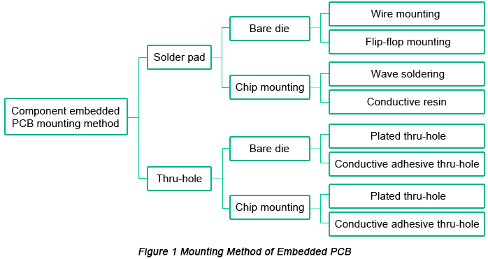
Currently, two embedded technologies applied to PCBs are available, which differ from each other in terms of mounting method. One depends on pad whereas the other on Thru-holes. The following figure demonstrates the main types of embedded PCB assembly methods and their subcategories.

When it comes to embedded component PCB with pad as a mounting method, firstly, embedded components should be assembled on electrodes formed on substrate and electrical connections are carried out. Afterwards, insulating resin is applied to fill and bury components and electrode. For mounting, SMT is depended. Solder or conductive adhesive is used as mounting material.
Component Embedded PCB Assembly Procedure
When component to be embedded is bare die, die bonding should be picked. If components are PDs, mould package, or Wafer Level Chip Scale Package (WLCSP), ultrasonic wave bonding, Controlled Collapse Chip Connection, Epoxy Encapsulated Solder Connection (ESC) and conductive resin etc should be applied. AD mounting, however, should take advantage of solder with wave solder or conductive resin.
Based on current manufacturing equipment and technological capabilities, the merits of pad as a mounting method include:
|
Mounting Method
|
Advantages
|
Disadvantages
|
|
Pad Mounting
|
• It is accessible;
• It features key technology with fewer difficulties;
|
• Its procedure is a little complicated;
• Process flow is needed from PCB fabrication to Surface Mount Technology (SMT) assembly;
• Embedded components need soldering, which increases risk of unreliability.
|
|
Thru-hole Mounting
|
• It contains few procedures;
• Embedded components don't need to go through soldering, which increases reliability of products;
|
•Its high complexity and immaturity, especially when it comes to microvia manufacturing and alignment technology of embedded components.
|
This article will discuss embedded technology involving pad as a mounting method.
In order to go for technological feasibility of ADs buried into a PCB and Surface Mount Devices (SMDs) embedment in PCB cavity, design and technological procedure research have to be firstly carried out. This article applies a double-layer embedded PCB with multiple packaging components as an example including Ball Grid Array (BGA), Chip Scale Package (CSP), and Quad Flat Package (QFP).
a. Trace Design
b. Manufacturing Procedure of Embedded PCB. Below image shows manufacturing process of substrate containing embedded components.

c. Embedded Components Assembly in Cavity. Components assembly in cavity is one of the top difficulties when it comes to embedded technology. On one hand, traditional planar pattern solder paste printing technology fails to be applied. On the other hand, during the process of wave soldering after successful mounting, gas inside cavity fails to be smoothly exhausted, leading to a high voidage of soldering. In order to solve the two issues, solder paste printing technique and vacuum wave soldering technique should be used with a manufacturing workflow indicated below.

Because mounting, plugging, cleaning and spray have been ordinary mature technologies, discussion in the rest of this article will center on solder paste printing technology and vacuum wave soldering technology.
• Full-auto solder paste printing tech features attributes of high efficiency and accuracy, it is applied to all types of complex and high-density PCBs.
• To implement wave soldering, the first step is to get vacuumized. As the intensity of pressure in vacuum cavity reaches a regulated vacuum degree, vehicle components start to be heated. Temperature of heating surface rises at t a speed of 0.5°C to 1.0°C per second from room temperature to peak temperature of wave soldering, that is, 200°C with this temperature maintained for 120 seconds. When solder is fully melt, pressure intensity inside vacuum cavity converts from vacuum conditions to atmospheric conditions. With hollow compression inside melting solder shrinking, temperature begins to go down.
Testing and Inspection
a. Soldering Quality Inspection - AXI will be applied to inspect soldering quality of embedded components buried in PCB. Inspection items include heat damage, burning, crack, scratch, fragmentation, fracture or other damage. Component mounting position and accuracy should be qualified. Solder surface should be guaranteed to be clean, smooth, void of crack, peeling, irregularity, fake soldering, cavity, desoldering, nonwetting and metal falling.
b. Electrical Test - a test programming should be designed to ensure all the circuits on board can successfully go through with power on.
c. Mechanical Intensity Test - it aims to test soldering intensity of components inside cavity.
d. Environmental Suitability Test - it only applies to products that will be applied in extreme environment. Environmental suitability test covers test environment ranging from extreme temperature, humidity to vibration and pressure in accordance with specific application conditions and demands.


