HDI, short for High Density Interconnection, is a type of printed circuit board technology starting to develop at the end of 20th century. For traditional PCB boards, mechanical drilling is utilized, with some disadvantages including high cost with aperture being 0.15mm and difficulty in improvement as a result of the influence of drilling tool. However, for HDI PCBs, laser drilling is utilized and as soon as it was introduced, it received massive popularity. HDI boards are also called laser boards whose aperture is ordinarily in the range of 3.0-6.0mil (0.076-0.152mm) and line width 3.0-4.0mil (0.076-0.10mm), which results in the fact that the pad size can be drastically decreased so that more layout can be arranged in each unit area. HDI technology adapts and pushes the development of PCB industry and now HDI circuit boards have been massively applied in all kinds of devices.
In terms of board design, compared with ordinary PCBs, the essential difference is that HDI PCBs obtain interconnections through blind holes and buried holes instead of through holes. Besides, finer line width and smaller spacing are used in HDI PCBs design so that the space for layout and track can be fully used. Therefore, HDI design novices must know how to arrange component space, how to switch applications of blind holes, buried holes and through holes, and how to distribute space for signal lines. Nevertheless, the first and uppermost job is to understand the corresponding process parameters in the HDI PCB manufacturing process.
• Aperture
Aperture ratio must be considered in through hole and blind/buried hole design. For traditional mechanical drilling used by ordinary PCBs, through hole aperture should be more than 0.15mm and board thickness-to-aperture ratio more than 8:1 (In some special circumstance, this parameter can be 12:1 or more). However, for laser drilling, the aperture of laser hole should be in the range of 3 to 6mil among which 4mil is advised and the plating filling hole depth-to-aperture ratio should be 1:1 at most.
The thicker the board is, the smaller the aperture is. In the process of plating, it's difficult for chemical solution to enter the depth of drilling holes. Although circuit plating devices press the solution to the center of drilling holes by means of oscillation or pressing, concentration gradient makes central plating relatively thin, which results in slight circuit opening on drilling hole layers. What's worse, when voltage increases or boards suffer impact in severe environment, defects become more obvious, which will finally cause circuit break and board failure. Therefore, PCB designers must fully know about the technique capabilities of PCB manufacturers before hand, or PCB fabrication difficulties will be added, scrap rate increased or even failure to fabrication.
• Stack
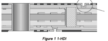
HDI PCB layer stack-up can be classified based on order of layers with blind holes. Here're some typical categories:
a. 1-HDI (with buried holes). Below figure shows the structure of 1-HDI with buried holes: 1-2 blind hole, 6-5 blind hole, 2-5 buried hole, 1-6 through hole.
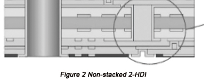
b. Non-stacked 2-HDI (with buried holes). The following figure shows the structure of non-stacked 2-HDI with buried holes: 1-2 blind hole (non-stacked), 2-3 blind hole (non-stacked), 8-7 blind hole (non-stacked), 7-6 blind hole (non-stacked), 3-6 buried hole, 1-8 through hole.
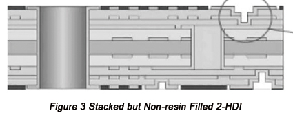
c. Stacked but non resin filled 2-HDI. Figure 3 shows the structure of stacked but non resin filled 2-HDI: 1-2 blind hole (stacked), 2-3 blind hole (stacked), 8-7 blind hole (stacked), 7-6 blind hole (stacked), 3-6 buried hole, 1-8 through hole.
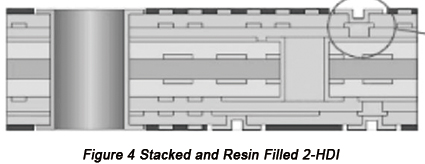
d. Stacked and resin filled 2-HDI. Figure 4 shows the structure of stacked and resin filled 2-HDI: 1-2 blind hole (stacked), 2-3 blind hole (stacked and resin filled), 8-7 blind hole (stacked), 7-6 blind hole (stacked and resin filled), 3-6 buried hole, 1-8 through hole.
Boards are usually influenced by pressure and temperature in the process of stacking up after which there is still stress in the boards. If stacked boards are asymmetric, that is, stress distribution on both sides of board is nonuniform, one-side warpage will be formed, drastically decreasing board yield. Therefore, designers must pick up asymmetric stack design and distribution of blind/buried holes must be considered.
• Process flow
Process flow will be discussed with 4-layer HDI with 1 stacking and 6-layer HDI with 2 stacking as examples.
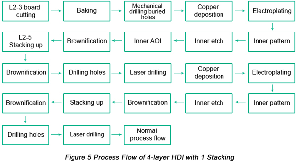
a. 4-layer HDI with 1 stacking. The following figure shows the process flow of 4-layer HDI with 1 stacking.
The process flow of 4-layer HDI is quite similar with that an ordinary PCB except the sequence of drilling holes. First comes mechanical drilling buried holes of 2-3 layer, then comes the mechanical through hole of 1-4 layer, then come 1-2 blind hole and 4-3 blind hole.
If designers directly drill 1-3 hole or 4-2 hole without 2-3 conversion just based on design requirement or performance, this design will bring extreme difficulties to fabrication, leading to the increasing of production cost and scrap rate. Therefore, when picking up method of through holes, present technique and fabrication requirement must be considered.
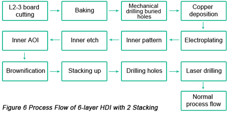
b. 6-layer HDI with 2 stacking. Figure 6 shows the process flow of 6-layer HDI with 2 stacking.
The process flow of 6-layer HDI with 2 stacking is similar with that of an ordinary PCB except the sequence of drilling holes. First comes mechanical drilling buried holes on 3-4 layer, then comes drilling of buried hole on 2-5 layer, then blind holes on 2-3 layer and 5-4 layer, then through holes on 1-6 and last come the drilling of 1-2 blind hole and 6-5 blind hole.
Laser drilling is used in blind holes on HDI boards and the high temperature in the process of laser drilling cauterizes the hole wall, which generates coke button that is absorbed on the hole wall. Meanwhile, the high-temperature cauterization will make the copper on the second layer oxidized. Therefore, after laser drilling, pre-operation should be implemented before electroplating. Because the aperture of blind holes is relatively small, it's difficult to eliminate the coke button. For 2-HDI, professional blind hole plating and filling must be required, which substantially increases the cost.
What's worse, the process flow of 6-layer HDI with 2 stacking needs some counterpoints so that the accumulated counterpoint errors will rise, and product scrap rate will rise. Therefore, 2-HDI isn't advised except for those extremely advanced products.
Component layout on HDI boards usually has such high density that it's necessary to ensure later installability, solderability and maintainability. The spacing between components can be determined based on the following table.
|
Components on HDI
|
Spacing
|
|
Ordinary SOP & PIN of other components
|
>40mil
|
|
BGA & PIN of other components
|
>80mil
|
|
PIN in ordinary components
|
>20mil
|
Parameters listed in Table 1 are limited values meeting ordinary soldering demands. In actual production , with the consideration of installability and maintainability, spacing should be enlarged as big as possible within the space to enable easy assembly, rework and soldering.
There are other aspects that need to be taken into consideration in terms of layout:
• RF/analog/analog-digital conversion/digital part must be strictly divided in space. Spacing between them should be enlarged no matter they are on the same side or different sides.
• Layout of the same module should be arranged on the same side in order to reduce the area of drilling or layer changing. So in the process of layout, key circuits must be determined and according to the significance level of signals, they should be arranged around key components.
• High-power signals should be arranged far from other signals.
Some elements must be taken into consideration in the process of tracking including the minimum line width, control of safe spacing and uniformity of track. If spacing is too short, clipping film can be caused in the inner dry film process. The residue of film will cause short circuit. If the line width is too small, the film has so weak absorption that open circuit will be caused. The nonuniformity of circuit will lead to the nonuniformity of copper thickness distribution and resin flowing speed at different points. Therefore, track and copper nonuniformity must be noticed in the process of design.
There are other aspects that need to be taken into consideration in terms of track:
• Components on Top and Bottom layers have relatively good isolation effect, so mutual crosstalk between inner layer signals should be decreased.
• For important signals in RF and analog areas, short ground-to-ground reflow path should be assured around each signal.
• Blind holes without physical connection interference mustn't be added to the track area of important signals so as to avoid the mutual interference but blind holes belonging to ground net can.
• Because of the limited space for tracking, it's first and foremost for the tracking space of important signals and signals with impedance requirements.
• On the premise of power's ability to meet current, monoblock pavement should be avoided in order to reduce the interference to other signals.
• If signal quality comes first, blind holes can be directly drilled on the pad. For BGA area, blind holes and pad can be kept tangent to avoid the influence to BGA soldering.
• Blind/buried holes are worse than through holes in terms of continuity. Therefore, for signals with impedance requirement, lead lengths between pad and blind holes, blind holes and buried holes should be shortened and upper and lower surface of signals should be complete.
In conclusion, in the process of HDI boards design, complicated manufacturability must be fully considered beforehand. Process parameters of regular PCBs have been familiar to most designers while HDI design novices should know about HDI PCB specification of custom circuit board manufacturers in order to ensure their projects.


