


PCB successfully added to your shopping cart
Design Issues on Thick/Heavy Copper PCBs for Military and Aerospace Applications
When electronic engineers are preparing for PCB design for military/aerospace (short form as "mil/aero") applications, some details and performance requirement have to be taken into consideration. It's generally known that both mil and aero products call for multiple operation conditions and a wide range of operating temperature. They have to be able to withstand multiple stringent environments with either extreme heat, like desert or extraordinary chill, like South Pole. Apart from extreme temperature, humidity is also a key consideration. As a result, in the process of designing PCBs for mil/aero applications, products' special working conditions have to be carefully considered such as temperature and humidity.
Reliability of military and aerospace products has been a main concern PCB design engineers must focus on. As a key aspect of products' reliability, shelf life has been regarded as a leading judgment standard. Take missile as an example. It isn't allowed to be exploded until it hits the target, which means that it has to normally run in a benign environment and features a relatively short shelf life. Engineers used to prefer reducing complexity of circuit boards applied for military and aerospace industries just due to high reliability of mil/aero products. Military and aerospace department would hesitate to know about new techniques of electronic product manufacturing until they had been proved to be feasible in corresponding industries. Currently, however, function requirement of mil/aero electronic products stops electronic design engineers from sticking to simple design ideas and experience only. Some of them have started embracing newly-emerged PCB fabrication techniques.
With the increasing of PCB techniques and complexity, electronic engineers have to concentrate on both PCB design rules and PCB manufacturing technologies so that products will reach an optimal balance between security, cost and performance requirement, leading to lowest manufacturing risk.
Successful PCB fabrication relies on frequent and smooth communication between electronic design engineers and manufacturing engineers, which has to be kept in mind. Design engineers should be fully aware of manufacturer's detailed capabilities such as trace width, spacing, pad size and via diameter etc. Furthermore, they have to take into account all requirements in terms of PCB type, material, thru-hole structure and power.
When it comes to mil/aero products design, engineers should conform to MIL standards. Other quality standards can also be applied as a reference. For example, IPC standard can be used for its inspection items and quality standard.
Currently, people tend to show a preference for high-speed transmission substrate material, which covers a wide range of performance parameter variation. In structures of more complex electronic products, data sheet provided by substrate suppliers can only indicate that some type of substrate material performs better than other types. Nevertheless, PCB manufacturer's experience can never be underestimated because to some extent, they are authentically aware of substrate material performance, especially in accordance with practical situations. For example, although PCB designers can figure out impedance of leads, different manufacturing methods will possibly lead impedance to be incompatible with design requirement.
Structure also plays an important role in mil/aero PCBs because it is able to help avoiding unnecessary cost or reducing risk resulting from complex structures. And for more complex mil/aero electronic products, their structures also influence manufacturability of products.
Historically, cost issue was seldom considered in military and aerospace electronic products. But it has to be admitted that increasing of product manufacturing cost would actually be beneficial to risk reduction in the process of manufacturing, which is, after all, worthwhile. In the procedure of PCB introduction, risk can be let down through increasing research and develop period and reviewing data integrity prior to manufacturing arrangement.
Thick/Heavy Copper PCBs for Mi/Aero Applications
• Definition
Mil/Aero electronic products with high power bring about new requirement to PCBs, which arouses the creation of thick/heavy copper PCBs or even extreme copper PCBs. Heavy copper PCBs refer to circuit boards whose conductor features copper thickness is within the range from 137.2μm to 686μm whereas circuit boards whose copper thickness is more than 686μm or reaches 6860μm are called extreme copper PCBs.
Structural advantages of heavy copper PCBs include:
a. Capable of withstanding heat stress with PCB's anti-stress capability enhanced;
b. Enhancing PCB carrying current capacity;
c. Increasing PCB thermal dissipation capability without need to assemble cooling fins;
d. Enhancing mechanical strength of layup between layers and plated-through holes;
e. Applicable for planar transformer with high power placed on board.
Each coin has two sides. Apart from those advantages, heavy copper PCBs feature some disadvantages as well. It's of significance to be aware of both aspects concerning structures of heavy copper PCBs so that how to make use of potential functions and applications can be clearly understood.
• Construction of Heavy Copper PCBs
Similar to Standard FR4 PCBs, heavy copper PCBs feature the same fabrication method with special etching and plating technologies applied, such as high-speed plating and deviation etching. For some time in the past, people once tried manufacturing heavy copper PCB with just etching. Some of circuit boards fabricated in this method suffered from scrap due to uneven edge lines and over-etching of margin. In order to avoid that, advanced plating and etching techniques were later applied so that straight edge and optimal margin etching could be achieved.
Plating on heavy copper PCB allows PCB fabricators to thicken both plated through-hole wall and thru-hole wall, whose advantages include:
a. Layer count shrinking;
b. Impedance distribution reduction;
c. Packaging minimization;
d. Manufacturing cost decreasing.
Heavy copper PCB can be seamlessly attached to ordinary board. When it comes to tracing and smallest spacing on circuit boards and range within tolerance and manufacturing capacity, they need to be determined by discussion between design engineers and manufacturers prior to authentic fabrication.
• Current Carrying Capacity and Temperature Rise
How much current is heavy copper PCB capable of carrying? This question usually depends on electronic design engineers. It includes copper thickness and width and maximum temperature rise heavy copper PCB is capable of withstanding determination. This question comes out like that since heat generated by heavy copper PCB in the process of running is closely related with current.
As current passes through wires, power consumption rate during running is 12% of original power so that lost power generates transition heat locally that will be dissipated into surroundings in a way of thermal conduction. The maximum current wires on heavy copper PCB can withstand has to be found out and a method to judge temperature rise and corresponding imposed current has to be dig out. According to guidelines of IPC-2221A, a formula indicating carrying current capacity by external wires is available: I = 0.048 x DT0.44 x W x Th0.725.
In this formula, I refers to current (unit: A); DT refers to temperature rise (unit: °C); W refers to line width (unit: μin); Th refers to trace thickness (unit: μin). Current carrying capacity of internal traces is 50% of that of external traces.
In conformity with the formula, Table 1 summed up current carrying capacity indicating carrying current at the temp of 30°C for different sectional areas.
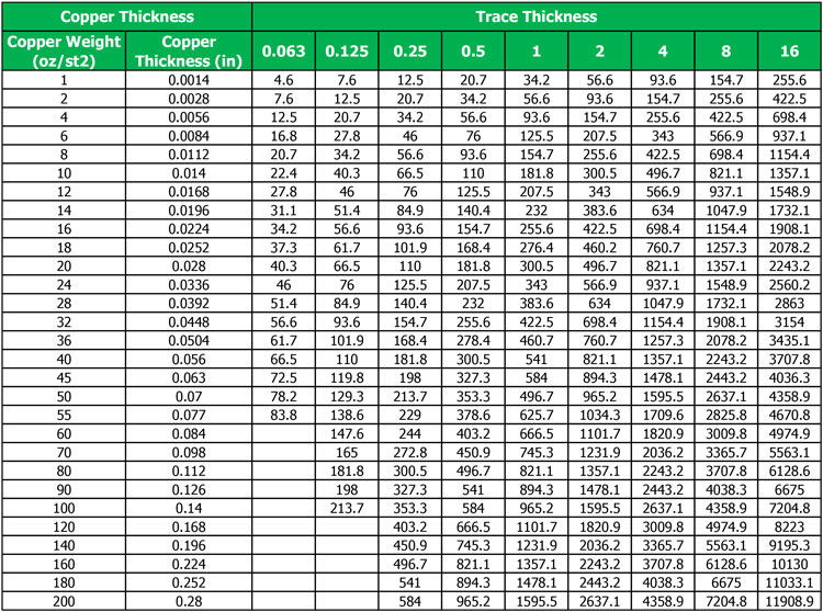
Table 1 Carrying Current (A) at a Fixed Trace Width (temperature rise is 30°C)
Substrate materials with different performances are available for PCB manufacturers and designers, ranging from ordinary FR-4 epoxy resin substrate material with an operation temperature 130°C to high-Tg substrate materials. Up to now, a set of methods have been developed to test heat-resistant quality of finished PCB products. Due to difference in terms of thermal expansivity between copper and substrate material, a "driving force" is created between them, that is, actually thermal stress possibly leading to crack, gathering and growing, which finally drives PCB to failure.
In the circulation test on through holes' capability to combat thermal shock, a set of 32 serial plated through holes is designed as a sample on the board and their situations will be checked after thermal shock test. The first failed plated through hole will be decided as the thermal stress a circuit board can withstand. Application of heavy copper PCBs in thermal shock circulation will reduce or eliminate failures.
• Thermal Dissipation Analysis
In the process of electronic components' running, high-power loss takes place in the form of heating that has to be generated by thermal source (components) and radiated to surroundings. Otherwise, components will suffer from over-heating or even failure. Heavy copper PCBs, however, are capable of dissipating heat more effectively than other types of circuit boards so that failure rate of boards will be dramatically decreased.
In order to make heat easily dissipated, a type of cooling fin is demanded to push heat dissipated into air through thermal conduction, radiation or convection. Usually, the other side of heat source of cooling fin is connected to copper area through copper plating through holes.
Generally speaking, ordinary cooling fins are connected with copper coating area on PCB through thermal conduction. There are also situations in which rivets or screws are used for connection. Most cooling fins are made of copper or aluminum.
Therefore, it is of much significance to assemble cooling fins during PCB fabrication, which can be achieved in heavy copper PCBs. Copper layer on the surface of circuit board can be thickened through electro plating, which improves heat-conducting property of board surface. Another advantage of this method lies in that thermal thru-hole copper plating layer can be thickened and thermal resistance of heavy copper PCB can be reduced.
It's such a long time since heavy copper PCBs have been employed to carry large-power components in military and aerospace industries that this type of heavy copper PCBs will be widely applied among different industries in the near future.
Helpful Resources:
• Thick Copper PCB And Its Fabrication Service
• Relationship between Copper Weight, Trace Width and Current Carrying Capacity
• The Key PCB Design Rules You Have to Know
• Full Feature PCB Manufacturing Service from PCBCart - Multiple Value-added options
• Advanced PCB Assembly Service from PCBCart - Start from 1 piece