



The quality of PCB assembly plays a crucial role in achieving manufacturing success, particularly as electronic devices continue to shrink, speed up, and get more complicated. Even a well-designed circuit may encounter production delays, soldering defects, or reliability issues if Design for Assembly (DFA) principles are overlooked during the PCB layout stage.
DFA is dedicated to maximizing the efficiency of PCB manufacture, inspection, testing and long-term reliability. Manufacturers can gain a competitive advantage by addressing assembly-related risks during the initial design phase to increase production yield, minimise rework, and accelerate time-to-market.
What is DFA (Design for Assembly) in PCB Manufacturing?
Design for Assembly (DFA) is the design of a PCB which is manufactured correctly, efficiently, and consistently. DFA takes many factors into account when dealing with assemblies such as:
The placement and space between components.
The design of the pad and footprint.The design of the pad and footprint.
Thermal management
Automated assembly compatibility
The access to inspection and testing.Access to inspection and testing.
The panelization and tooling support are provided.
DFA is related to Design for Manufacturability (DFM). DFM is primarily responsible for fabrication needs, whereas DFA will specifically consider optimizing assembly and prevent defects.
Proper implementation of DFA by manufacturers can give them:
Higher first-pass yield
Decrease in assembly defects
Reduced production delays
An increase in the reliability of the solder joint.
Lower manufacturing costs
Common DFA Errors and Their Solutions
Component Placement and Spacing Problems
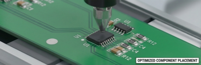
One of the most frequent reasons for PCB assembly failures is when components are installed incorrectly. The proximity of components can pose problems for automated pick and place machines, soldering equipment, and apparatus for inspection. High-density layouts also lead to solder bridging, concentration of heat and rework problems.
ICs, LEDs, diodes and capacitors are examples of components that are commonly polarized, and if not oriented correctly, can lead to further assembly and automated optical inspection issues.
How to Fix It
Follow IPC recommended personal space.
Provide adequate clearance for soldering and inspection.
Arrange polarised parts in the same direction.
Don't put tall parts too near small SMD devices.
Maintain clear and readable silkscreen markings.
Optimized placement of parts increases the efficiency of assembly and minimizes assembly error.
Footprint, Pad and Via Design Errors
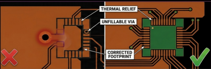
Another leading reason for assembly failure is incorrect PCB footprints. Weak soldered joints, open circuits and component misalignment can be caused by incorrect pad sizes, pin spacing or a library of outdated components.
Other soldering problems like solder wicking, uneven distribution of solder and lack of thermal balance can also be caused by poor pad and via design. The via in pad structures, which are not completely filled, present a special challenge in high-density designs.
How to Fix It
Confirm footprints with most up to date component datasheets.
Apply land pattern standards that meet IPC requirements.
Check custom footprints prior to production.
Use filled or capped vias as necessary.
Use correct temperature relief patterns.
Properly balance copper around pads.
Right pad and footprint design provides a stable solder joint and quality assurance of assembly.
Thermal Management and Reflow Issues
Tombstoning, cold solder joints, shifting of parts, PCB warpage are just some of the defects that can happen during reflow soldering due to the distribution of heat. Thermal instability is often caused by large pours and bad layer stackups.
The risk of board deformations during heating cycles can also be high if the structure of the PCBs can be thin and the copper balancing is not good.
How to Fix It
Evenly distribute copper over all PCB layers.
For large copper surfaces use thermal reliefs.
Tune reflow temperature profiles.
Ensure symmetrical PCB stacking.
Do not over-thermalize a local area.
Thermal management can enhance the reliability of solder joints and overall stability of the assembly.
Missing Fiducials and Poor Panelization
Fiducial marks are critical reference points used by automated pick-and-place systems. Inaccuracies in placement are caused if fiducials are missing or misplaced, particularly for fine pitch components and BGAs.
Meanwhile, bad panelization assembly can lead to the instability of handling while assembling. PCB flexing and/or mechanical damage can occur during depanelization due to weak breakaway tabs, lack of tooling rails or poor board support.
How to Fix It
Make global fiducials on every PCB panel.
For fine pitch components use local fiducials.
Be careful not to have solder mask interference with the fiducials.
Provide adequate tooling strips and support rails.
Apply suitable V-scoring or tab-routed techniques.
Provide board stability during reflow.
Precise assembly and manufacturing, through good panelization and alignment.
Testability and Documentation Problems
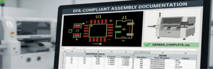
Electrical testing is more difficult and debugging time is longer during production because of the lack of test point accessibility. Meanwhile, design-to-manufacturing documentation can be incomplete, leading to communication problems between design and manufacturing teams.
Typical documentation issues are wrong pick and place data, incomplete assembly drawings, wrong polarity indication and wrong BOM files.
How to Fix It
Provide easily accessible test points on important signals.
Follow spacing requirements for test probes.
Allow for access to test points following assembly.
Supply full BOM and Gerber.
Add correct assembly drawings and centroids.
Polarity and orientation are clearly identified.
Better testability and documentation leads to lesser manufacturing confusion and reduces troubleshooting time.
Best Practices for Preventing DFA Errors
In order to boost the assembly performance and decrease production risk, PCB designers should:
Verify footprints carefully
Ensure correct spacing of components
Standardize component orientation
Optimize thermal management
Include fiducials and tooling features
Design for automated inspection and test.
Improve documentation accuracy
Perform DFA and DFM reviews early in design, development, or manufacturing process
A proactive DFA approach will help lower manufacturing costs, increase product reliability and production efficiency.
One of the major contributors to PCB assembly defects and delays is DFA errors. Issues like component placement, footprint design, thermal imbalance, panelization, and documentation can have a significant effect on the quality of the assembly, and overall efficiency of the production.
Incorporating DFA concepts at the PCB design phase can minimize the chance of assembly failures, enhance first pass yield and ensure more dependable electronic products. Stable and cost-efficient PCB assembly requires effective collaboration between designers and manufacturers. PCBCart has extensive PCB assembly and manufacturing knowledge and excellent DFM/DFA engineering capabilities, which can help customers optimize their designs for efficient and high-quality electronics manufacturing.


