.png)
.png)


PCB successfully added to your shopping cart
PCBCart Thailand Factory—Fully Prepared for Production! Learn More

 English
English
English
English
English
 Español
 Deutsch
 Français
 Italiano
 日本語
日本語
 ภาษาไทย
 Malay
Malay
Your First PCB Assembly Order
PCB Assembly Cost $500OFF
Coupon Code: FCPCBA
Applicable to turnkey PCB assembly services only. Other restrictions
may apply.
.png)

.png)
.png)
Product Portfolio &
PCB Assembly Services
IPC610-D Standards
ISO9001 Quality products
Over 99.8% Satisfaction rate
Under 0.1% Complaint Rate
PCB Manufacturing and Assembly
Services All in One Place

25,000+
different part numbers
delivered annually
100,000+
served customers in
120+ countries
Box Build Assembly
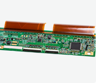
Rigid Flex PCB Assembly
.png)
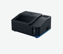
High Frequency PCB Assembly
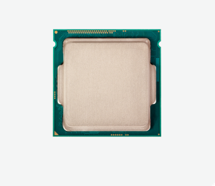
BGA Assembly Services
.png)
.png)
.png)
.png)
Just like the PCB business, our PCBA services at PCBCart are tailored
for prototyping, low-volume, and high-volume production, making us your
true one-stop solution for PCB fabrication and assembly. This integrated
approach streamlines your R&D, shortens lead times, and ensures
consistent quality. Backed by a professional engineering team, we
support you from design to delivery with services like free DFM/DFA
checks, BOM optimization, and functional testing. Fulfilling global
orders daily, PCBCart has built a reputation for high efficiency,
certified quality, and cost-effective solutions. Our ISO 9001 and IPC
Class 2/3-compliant factory is equipped with advanced systems and
inspection tools—such as AOI, X-ray, and functional test systems—to
guarantee reliable results from prototypes to full-scale production.
PCBCart Assembly Capabilities: SMT, THT, Mixed Technology, BGA, POP,
Rigid & Flex PCBs, Box Build, Full Turnkey, Partial Turnkey, Kitted
Assembly, Cable & Wire Assembly. Compliant with ISO 9001 and IPC 610
Class 2 & 3 standards.
Order Process
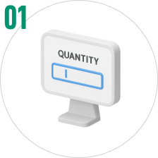
Fill in the quantity to get a quote for PCB assembly online.
Please upload your BOM file and PCB Gerber file so that we can quote you
faster and more accurately.
We will confirm the details (testing or programming) with you before
production. If you have any questions or need more information, please
feel free to contact your dedicated customer service.
Top Question
PCB Panels
Tolerances
PCB Expedited Service
Blind Via and Buried Via
Layer Stackup
PCB Materials

Our PCB Assembly Solutions
PCBA
PCBCart offers turn-key PCB assembly services for prototype to
high-volume production, handling everything from component sourcing
and PCB fabrication to assembly, testing (including AOI/X-ray), and
final shipment, with capabilities including SMT, THT, mixed assembly,
BGA, POP, and RoHS-compliant processes.
PCB Fabrication
PCBCart offers a comprehensive solution that covers both PCB
manufacturing and prototype assembly, with a strong emphasis on
low-volume production and circuit board prototyping. We excel at
delivering high-quality, budget-friendly printed circuit boards,
including sophisticated multilayer designs reaching up to 14
layers.From impedance-controlled PCBs to boards featuring blind or
buried vias and intricate multilayer structures
PCBA Process
.png)
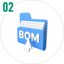
Before assembly begins, all incoming materials,
including fabricated PCBs and electronic components,
undergo rigorous quality control checks.
including fabricated PCBs and electronic components,
undergo rigorous quality control checks.
· Accurate resistance and capacitance values
· Consistency between component pads and the board
· Precise incoming quantity verification
· Detection of any abnormal components
· Consistency between component pads and the board
· Precise incoming quantity verification
· Detection of any abnormal components
.png)
A crucial step in the surface mount PCBA process flow, solder paste
printing involves applying solder paste to a printed circuit board
(PCB). The most common method utilizes a stencil printer to
accurately deposit the correct amount and thickness of solder onto
the solder pads.
.png)
Solder Paste Inspection (SPI) aims to identify defective solder
paste printing early in the Printed Circuit Board (PCB) assembly
process. SPI directly assesses the quality of solder paste on the
PCB, helping to significantly reduce defect rates and save
considerable cost and time.
.png)
Component placement is an electronic manufacturing PCBA process that
precisely mounts surface-mounted devices (SMDs) onto designated
locations on a printed circuit board (PCB). This step is essential
for establishing electrical interconnections between the components
and the PCB.
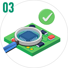
Manufacturers utilize Pre-Reflow Automated Optical Inspection (AOI)
to rapidly identify and address any defects before the PCBA
production moves to the next phase. This strategic inspection point
is vital for ensuring a reliable and efficient assembly process.
.png)
The reflow soldering process temporarily attaches electronic
components using solder paste. Through a controlled high-temperature
profile, the solder paste melts, allowing the surface-mounted
components to be firmly adhered to the PCB board.
.png)
Post-Reflow AOI can detect mis-soldering, reverse soldering, empty
soldering, empty soldering, lack of penetration, short circuit,
offset, tombstone, etc. after reflow soldering. It can also detect
defects such as excessive welding, insufficient welding, and
continuous welding in the appearance of PCBA solder joints.
.png)
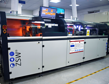
PCBA through-hole component soldering is a vital step. Manual
soldering offers flexibility and precision for small batches and
prototyping, though with lower productivity. Wave soldering, on the
other hand, is ideal for mass production due to its high efficiency
and consistency, but it has limitations in component selection,
requires preheating, and can be more costly.
.png)
The first sample test involves cross-referencing the completed PCBA
with Gerber, BOM (Bill of Materials), and coordinate files. A
first-sample tester re-verifies the resistance and capacitance
values to confirm the accuracy of all parameter values.
.png)
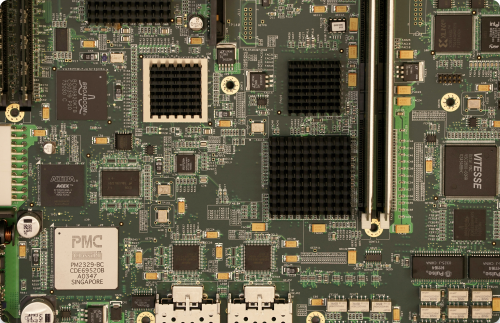
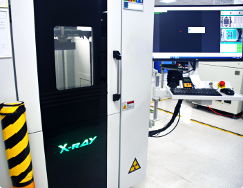
X-ray inspection is commonly performed on Quad Flat No-Lead (QFN)
and Ball Grid Array (BGA) components during printed circuit board
assembly. This process checks the solder joints of otherwise
invisible components, ensuring the reliability of each solder ball
in a BGA.
.png)
The ultimate stage of the PCB assembly process is the final
inspection and functional test, which verifies that the PCB operates
as intended. Additionally, specific applications may have further
requirements. For example, automotive PCBs might undergo drop tests,
while medical PCBs may require halogen testing.
PCB Assembly Facilities Showcase
Advanced Equipment and Testing
Main Products
Jet Printer and Dispenser (MYCRONIC)
Main Products
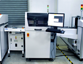
3D AOI
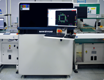
Main Products
High-Speed 3D Solder Paste Inspection System
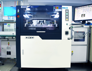
Main Products
High-Precision Solder Paste Printer
Main Products
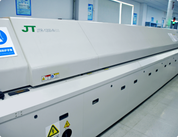
JTR-1200D-N Reflow Oven
Main Products
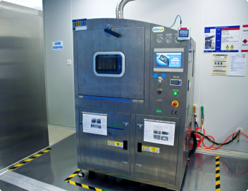
KED600 Batch Cleaner
Main Products
SE-450-HL Wave Soldering System
Main Products
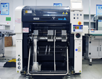
Panasonic NPM-W2 Chip Mounter
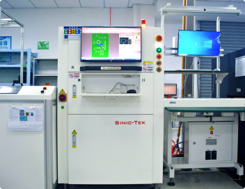
Main Products
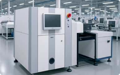
X-RAY
Main Products
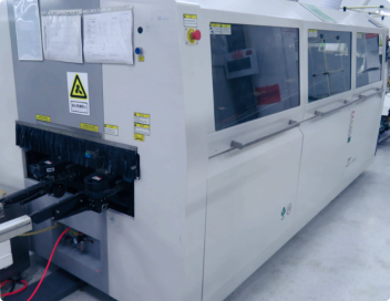
ZSWHPS-11-2 Selective Wave Soldering Machine
Contact us
- Singapore Headquarter: SOTATRONIX PTE.LTD
-
 [email protected] [email protected]
- Thailand Factory: Sota Electronics Co.,LTD
- Add: Asia Industrial Estate, Samut Prakan Province, Thailand
- China Factory: GENERAL CIRCUITS CO., LTD
- NO.163 Wu Chang Avenue, Yuhang District, Hangzhou, China
Subscribe
Capability
- Quickturn PCB Prototype
- Full Feature PCB Manufacturing
- Advanced PCB Assembly
-
Electronics Manufacturing
Services - PCB Layout