Preliminary stage. Now, boards with no components assembled on the surface of board are called bare boards. More than four decades ago, soldermask didn't exist and copper lines were exposed to the air. Put in another way, this type of finished PCB is actually an exposed bare board. In this stage, components were assembled on PCB through lead plug-in soldering. Pad of PCB is a copper surface and solder wire with rosin core is applied to be soldered by soldering iron. Later, flux is coated on the whole PCB surface in order to protect circuit and solder pad and the coating method is mostly through flux of rosin and resin spraying. Of course, chemical silver plating is applied sometimes.
Primary stage. Since 1970s, PCB depended on flux to protect its circuit and passivation treatment was applied to stop copper oxidation by surface finish on pad, which aims to stop copper surface from oxidation. Solderability, however, was insured by second-time flux coating in the process of assembly. Then, some other types of surface finish came into being such as chemical gold plating, chemical tin plating, electroplated soldering and hot melting tin soldering and some products with high reliability applied electronickelling and electrogilding.
Maturity stage. At the beginning of 1980s, HASL started to be applied to take place of electroplated soldering and hot melting tin soldering. Meanwhile, OSP took place to substitute passivation treatment stopping copper surface oxidation and flux treatment with rosin coating. In the middle of 1990s, ENIG took off and ImAg and ImSn became mature as well.
Improvement stage. Advent of 21st century has witnessed new requirement on surface finish owing to the development of PCBs. In order to conform to RoHS regulations and implement lead-free PCB Assembly, electroplated tin lead alloy has to be totally eliminated and HASL containing lead has been reduced increasingly, replaced by lead-free HASL or other types of surface finish. With the development of PCB towards high density and fine spacing, pad space has to be fine and surface finish be smooth so as to adjust micro mounting component soldering assembly and chip metal line assembly so that application of lead-free HASL is being reduced. Performance of existing OSP and ENIG is improving as well and ENEPIG becomes pervasive. Requirement of high density and high frequency of PCB leads to advent of new nickel-free coating.
Up to now, diversity of application market of PCB leads to diversity of surface finish requirement and suitable surface finish and requirement should be selected based on different applications.
• OSP
OSP, short for Organic Solderability Preservative, refers to a thin film that is formed at the surface of bare copper in a chemical method. This film features oxidation resistance, thermal shock resistance and anti-wettability, more suitable for developing requirement of SMT in electronic industry.
The main content of OSP is organic substance containing heterocyclic nitrogen such as alkylbenzimidazole, BTA (benzotriazole), benzimidazole etc. An organic film is coated on clean copper surface of PCB pad and through-hole via through complexation and cross-linking reaction. The key ingredient of OSP solution determines solderability and thermal resistance of PCB that can be illustrated from color changing state due to heat and film decomposition temperature, which is extremely significant to the soldering performance of surface mounting,
Thickness of OSP film should be in the range from 0.2μm to 0.5μm, neither too thick nor too thin. Otherwise, it fails to stop copper surface from oxidation if it is too thin while flux fails to totally dissolve OSP plane on copper surface in the process of assembly, which will lead to bad soldering instead.
The responsibility of OSP is to cut off humidity in order to stop oxidation of copper surface, to beat against high temperature and maintain activation and it can be easily melted by flux so as to keep excellent tin plating capacity. Furthermore, different from physical coating, OSP features such excellent selectivity that contaminant won't be generated on soldermask, carbon film or gold side.

Here are advantages of OSP surface finish:
1). Suitable for PCB with SMT and fine line space;
2). Capable of stopping copper surface from oxidation, suffering repeated
heat shock and compatible with multiple solder and easy for soldering;
3). Beneficial to smoothness of PCB;
4). Environment friendly;
5). Contributive for low cost;
Of course, OSP film is so thin that it's easy to be scratched and engineers have to be very careful since once film is broken, solderability won't be insured. Furthermore, PCB with application of OSP as surface finish has to be stored in the environment at dry room temperature without aggressive gas (usually 15°C to 25°C, ≤60%RH). Moreover, storage span won't be more than three months.
• HASL
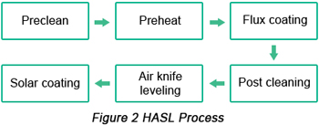
HASL, short for Hot Air Solder Leveling, refers to dipping PCB into melting solder bath and then redundant soldering tin is blown away from PCB surface or metalized via through hot wind so that a smooth, uniform and bright soldering tin coating can be obtained. As users' requirement on PCB with flux coating on bare copper increases, HASL receives fast development.

Boards have to meet the following requirement after HASL:
1). All solder coating layers have to be smooth, uniform and bright with no defects such as knot or exposing copper. In addition, soldermask can never suffer from bubbles, falling off or color changing and copper under soldermask should never be oxidized or change color. There shouldn't be foreign matters on the surface of PCB or in via and soldering tin shouldn't be there either.
2). Thickness of soldering tin layer should be in the range from 3μm to 8μm with overall covering soldering tin layer and solderability as principles.
3). Traditional soldering tin layer containing lead is increasingly be cancelled and lead-free soldering tin with tin as core, coupled with infinitesimal copper or nickel. The key is to maintain solderability. Melting point of lead-free solder tin is higher than that with lead by 30°C so heat resistance of substrate material and reliability of through-hole vias on the board will be challenged.
The essential advantage of HASL lies in solderability. This type of solder tin is basically the same as assembly solder and they are united through mutual melting when soldering. However, disadvantages of HASL are so obvious that coating features bad smoothness and temperature is so high that PCB performance will be influenced. With the escalation of high density circuit design, micro component assembly requires a smooth surface and otherwise, connection reliability will be affected. Moreover, PCB with high density is designed to be so thin that material fails to suffer from being dipped into high temperature melting material. Therefore, HASL is on a difficult way.
• ENIG
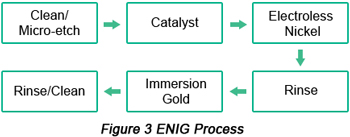
ENIG, short for Electroless Nickel and Immersion Gold, refers to first deposition of nickel layer and then gold layer on copper surface of PCB through chemical electroplating. Chemical nickel player and gold layer have been massively applied owing to their advantages including good dispersibility, solderability, wiring bond performance, soldering performance and their compatibility with all kinds of flux. Compared with OSP and HASL, ENIG is capable of meeting multiple assembly requirements with functions of solderability, connection, wiring and heat dissipation. Moreover, both board surface and SMD pad are smooth, suitable for fine lines.

Chemical nickel plating layer is actually a Ni-P alloy containing phosphorus whose content is in the range from 7% to 9%. PH value and stabilizer in solution play a significant role in determining content of phosphorus in plating layer so it's necessary to control PH value at about 5.1. Thickness of nickel layer is required to be more than 3μm, determining reliability of ENIG.
Immersion gold on nickel surface is actually a replacement reaction. In principle, when nickel surface is totally covered by copper, gold precipitation will stop. However, as a result of too many holes on the surface of gold layer, nickel under gold with multiple holes will still be dissolved and gold will still continue to be precipitated on nickel with an increasingly low speed until it stops. Immersion gold layer features thickness in the range from 0.03μm to 0.1μm. Copper only plays a role in protecting nickel layer from oxidation and dialysis. However, thickness of copper can't be too high, since otherwise, breakdown will take place in terms of brittleness and insecurity.
ENIG is simple to operate without need of technical leads. But black pad will possibly take place in the process of soldering, leading to reliability issue. The reason for black pad lies in the fact that immersion gold is a replacement reaction and nickel layer is partially dissolved and eroded by gold solution. Then metal compound is generated between nickel and gold layer and contaminated on this layer. Long storage span of PCB will cause color change of gold layer or black pad as a result of heating.
Now that black pad is occurred as a result of nickel layer corrosion, how to reduce nickel corrosion lies in control of phosphorus content. Besides, gold content has to be controlled in immersion gold solution, which helps to decrease nickel corrosion. In addition, change of additive and some operation parameters is also capable of helping to decrease black pad.
Up to now, immersion gold solution contains cyanide in it. Since it is an extremely toxic substance that greatly influences environment and people's health, it is suggested that cyanide will be applied less or won't be applied at all.
At present, ENIG is still an important type of surface finish and new nickel coating solution has been developed, which is capable of effectively controlling stability of solution and decreasing brittleness of nickel layer for more flexibility. PH value of new type of immersion gold solution tends to be neutral with gold content greatly decreased, leading to obvious reduction of cost and corrosion.
• ENEPIG
ENEPIG, short for Electroless Nickel Electroless Palladium and Immersion Gold, completely aims to prohibit the production of metallic compound between nickel and gold layer through participation of a type of stable mental layer, palladium, between nickel and gold layers. Palladium layer totally stops nickel migration and production of new compound, effectively avoiding black pad that occurs in ENIG.
ENEPIG, as a type of surface finish, integrates advantages of other types of surface finish such as solderability, wirability, smoothness, oxidation resistance, heat resistance and long-term reliability, so it is regarded as "versatile" surface finish by the industry.
In the process of application of ENEPIG as a surface finish, palladium is added to original nickel plating immersion gold, calling for a palladium plating tank in the original production line. As a result, cost can be saved. From the perspective of cost of metal material, reduction of gold layer thickness leads to lower cost of nickel/palladium/gold coating than that of nickel/gold coating.
Progress from ENIG to ENEPIG surface finish is beneficial to ensure reliability after component assembly. Based on analysis on palladium layer in ENEPIG, it can be demonstrated that palladium layer is composed by pure palladium and palladium-phosphor alloy with different hardness. Therefore, different palladium layers should be selected in accordance with requirement of wiring bonding or plating. What's more, thickness of palladium should be just right because existence of micro palladium will increase copper-tin production thickness while too much palladium will strengthen brittleness of palladium-tin alloy, which then will decrease soldering intensity.
• Nickel/Gold plating
As a traditional technique in PCB, nickel/gold plating is majorly applied in surface nickel/gold plating of plug at the side of PCB or switch contact, playing a role in improvement of abrasion resistance and conductivity or applied in nickel/gold plating at the surface of circuit and pad, playing a role in protecting copper layer and improving reliability of plating or wiring connection.
Advantages of nickel/gold plating are displayed as simplicity in terms of control and quality insurance. However, the foremost disadvantage is that it has to depend on technical leads to ensure certain plating connection between terminal points and nickel/gold. Technical leads adding and elimination increases amount of work and isn't suitable for PCB with high density. Therefore, this type of surface finish receives increasingly fewer applications.
• ImAg and ImSn
Both ImAg (Immersion Silver) and ImSn (Immersion Tin) are traditional techniques. At the beginning of their development, they receive few applications due to their bad stability and reliability. At present, with the progress and improvement of ImAg and ImSn, both surface finishes maintain being applied in PCB. Put in another way, both techniques are constantly improving with their own attributes.
a. ImAg
Silver is good conductor with excellent conductivity and surface of silver is smooth and solderable, beneficial to signal transmission integrity. However, silver is so sensitive to environment that it tends to change into yellow through chemical reaction and when oxidation layer becomes black, solderability will definitely be influenced. In order to avoid such situations, on one hand, storage environment should be improved and storage times be reduced. On the other hand, micro amount of organic matters should be contained in silver layer so that oxidation will be stopped.

Here are attributes of ImAg surface finish:
1). Excellent solderability, relatively high wetting ability and capable of
meeting requirement of multiple reflow
;
2). Suitable for wiring bonding and pressure contact technology;
3). Even coating and high smoothness of surface, suitable for fine space
assembly
;
4). Excellent conducting performance and reliable bonding;
5). Low operation temperature, suitable for thin boards;
6). Relatively low cost;
b. ImSn
As a major element of solder, tin coating features smooth surface and excellent solderability. The foremost disadvantage of ImSn lies in tin whisker generation as a result of migration between copper and tin, influencing reliability of PCB and prohibiting the development. However, with the increasing mature technology of tin, special additive has been developed to stop tin whisker from being produced.

In the process of manufacturing, tin surface tends to become black because tin surface tends to be oxided so easily that high acidity of water cleaning after immersion tin leads to black tin surface with oxidation. Moreover, contaminant of acid solution on transmission roller also tends to become black as a result of oxidation. Tin thickness is greatly correlated with temperature instead of tin concentration, acidity, thiourea concentration and additive.
Here are attributes of ImSn surface finish:
1). Excellent coplanarity of coating;
2). Even coating thickness distribution;
3). Lead-free
;
4). Capable of suffering from multiple soldering;
5). Low operation temperature;
6). Relatively low cost;
• New types of surface finish
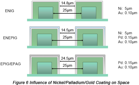
With PCBs developing towards high density and high performance, some present surface finishes fail to meet all requirements. Take fine space circuit diagram as an example. When space is 25μm between adjacent two pads and conventional ENIG or ENEPIG are applied, space will be decreased to about 15μm. When reduction reaches 40%, circuit accuracy and insulativity will be influenced. This can be displayed in the following figure.

Furthermore, nickel features bad conductivity that is about one third of that of copper and nickel features ferromagnetism that obviously leads to increasing of signal loss. However, OSP, ImAg and ImSn have no evident influence on signal loss.
In accordance to the problems occurred by ENIG and ENEPIG, here are some solutions.
a. EPIG or EPAG
Due to the bad influence of nickel layer on fine circuit and high-frequency signals and nickel's complete inadequacy, thin ENEPIG is applied as a solution to disadvantages of ENIG and ENEPIG. Chemical palladium/gold plating is applied to replace ENIG and ENEPIG. Without the participation of nickel, surface finish becomes so thin that deformation won't be generated to circuit. Moreover, high-speed signal transmission loss is decreased as well.
A variation of ENIG is EPIG (Electroless Palladium/Immersion Gold) whose palladium layer is 0.1μm thick and copper layer 0.1μm thick. Through experiment and test, EPIG is concluded to be with good reliability and expansibility.
Another variation is EPAG (Electroless Palladium/Autocatalytic Gold) with the thickness of palladium layer 0.15μm and copper 0.1μm, suitable for wiring bonding of gold lines and copper lines. Advantages of EPAG include better high-frequency attribute, suitable for fine space circuit as a result of thin coating, reliable soldering or wiring bonding and reduction in procedure and cost.
b. Electroless nickel ImAg (Ni/Ag)
In spite of low cost and excellent solderability of ImAg, it tends to be easily oxidized owing to its bad anti-corrosion capability. As a result, some improvement has been done with Ni/Ag introduced. Nickel features good conductivity and solderability while nickel has anti-corrosion capability.
With similar technology with ENIG and ImAg, Ni/Ag is developed from practical perspectives. Ni/Ag features palladium thickness in the range from 2μm to 6μm and that of silver 0.1μm.
c. HASLEN
HASLEN is the combination between HASL and electroless nickel. Usually, nickel is difficult for wetting and plating as a result of oxidation when it's exposed to air, so liquid flux is developed based on DES. Compared with HASL, the advantages of HASLEN include: a nearly unlimited life span as a result of higher anti-oxidation reliability; higher reliability owing to its high temperature resistance; avoidance of black pad; low cost.
d. SENIG/OSP
Electronic package arouses a lot of requirements on PCB surface finish. Miniature and lead-free trend of electronic assembly put higher requirements on surface finish, which is why SENIG/OSP occurs. This type of technology is complicated in that after the formation of PCB pattern and soldermask pattern, imaging is implemented to protect copper surface for OSP and expose copper surface for ENIG after which photo-induced resistant layer is eliminated to complete OSP. The key point of these technologies lies in corrosion resistance of electroless nickel layer.


