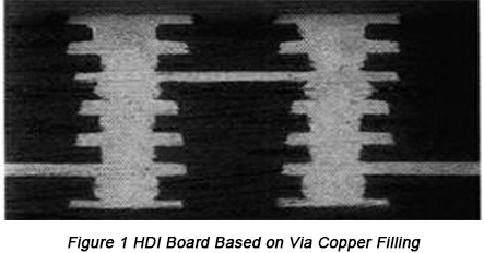
In recent years, with the fast development of electronic products concerning digital video and digital mobile communications, the development in this type of products is pushing PCBs towards the development in terms of lightness, thinness, miniature, multiple functions and high density and reliability. The limited routing space on PCBs leads to the close limiting between vias, wires, wires and vias and the advent of via copper filling craft, making the density of PCBs improve by approximately 10% to 30%. Figure 1 shows a HDI (High Density Interconnection) board based on via copper filling.

Since via design is capable of saving routing space to a great extent and blind vias filled with copper feature high reliability, blind vias with copper filling plating have a lot of advantages. In addition, this craft is relatively simple, cost saving and holds simplified procedure. Due to those merits mentioned above, blind via with copper filling plating will be massively applied in HDI PCB fabrication, regarded as an upcoming trend in the field of PCB. However, some problems still take place with the application of blind via with copper filling plating including extremely large dimple, leakage and empty cave inside vias. As a headache for PCB manufacturers, lots of complicated elements contribute to empty cave inside vias. This article will discuss the causes for empty cave inside vias and bring about corresponding measures to deal with them in order to solve the failure and increase the yield of products.
Failure Analysis
A lot of elements cause empty cave in blind vias with copper filling plating and each element has to be analyzed from the perspectives of characteristics and forming mechanism so that effect will be optimized.
• Bubbles in blind vias
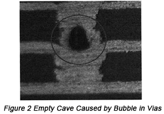
The sources of bubbles derive from external bringing in and self reaction. Generally, flash plating is required to be processed on PCBs prior to copper filling plating in order to strengthen via conductivity and be convenient for storage. Serious via oxidation tends to be caused if boards stay exposed to the air for a long time, so dwell time should not be too long. Put another way, bad preprocessing will lead to unelimination of bubbles in vias and oxidation plane, greatly increasing the rate of empty cave in blind vias, which is indicated in Figure 2.

The advent of bubbles also lies in anodic reaction in copper tank and the reaction H2O → 1/2O2 + 2e- + 2H+ will take place on anode when insoluble anode is applied. Based on this reaction, it can be concluded that oxygen will be escaped from insoluble anode, leading to high additive compensation and escalation of life span of anode or even passivation of anode and PCB defect. Therefore, to solve this problem, moderate ferrous sulfate is added into plating solution to eliminate the oxygen escaping from anode when anode reaction follows these two reactions: Fe2+ → Fe3+ + e-, Fe3+ + Cu → Fe2+ + e-.
To ensure smooth implementation of reaction, Cu has to be constantly added into plating solution, generally cupric oxide powder. Simultaneously, to reduce the parasitic reaction on cathode, higher requirements have to be set in terms of flowing in plating solution and cathode material has to be improved.
This type of failure caused by empty cave usually takes place at the bottom of blind vias, displaying symmetrical and regular shapes. For the improvement of this problem, measures can be carried out from the following aspects:
a. Dwell time and storage environment must be well controlled prior to copper filling plating. Commonly, for boards without flash plating, copper filling plating has to be finished in 4 hours while for boards with flash plating completed it has to be finished in 12 hours. Boards should be stored far away from acid environment and if possible, it's best to store them in rooms with air conditioners capable of controlling temperature and humidity of the room.
b. Preprocessing effect should be improved and necessary bubble elimination devices should be added. Preprocessing is extremely significant since preprocessing copper filling plating is directly related with filling effect. To ensure preprocessing effect, acid degreasing agent is advised to be picked up and the amount of water flow is suitably increased. Moreover, in winter when water temperature is relatively low (less than 15°C), a little sulphuric acid should be added for water washing after the application of degreasing or heating devices can be added to ensure the washing effect. Furthermore, vibration and air poppet valve can be assembled on preprocessing tank in order to eliminate bubbles in vias.
c. Selection of anode material of copper tank and control on current parameters. Based on the second source of bubbles, it's very important to select suitable anode material of copper tank. Anode material should be helpful for the improvement of anode performance and decreasing of additive consumption. When current parameters are too large, reactions on anode will be accelerated so that the number of bubbles will be increased. Under such condition, bubbles will enter blind vias as they flow out and can't be eliminated away from vias. Therefore, apart from the selection of anode material and control of current parameters, anode bag or protection layer are required to be added to the outside of anode net in order to prevent bubbles generated by anode directly entering plating solution.
• Imbalance of additive components
The components of copper filling plating solution include copper sulfate, sulphuric acid, chloride ion and additive and filling effect inside blind vias is implemented through the mechanism of action between components in plating solution. Additives play their own roles in the process of plating mutually and independently. Brightening agent plays a role in absorbing characteristics or electric features on electrode interface and changing sediments form and property to obtain the required prospective plating plane. Delivery agent is capable of pushing brightening agent to move forward each distribution of cathode dimple. However, it won't work unless chloride ions help. Delivery agent is responsible for making uneven distribution become even due to its capabilities of leveling ability and even plating ability. Leveling agent tends to be absorbed by positions with relatively strong electronegativity because it features strong electropositivity in acid solution. Then, it makes copper ions difficult to deposit without the influence of copper deposit in density area with low level as a result of competition with copper ions with positive electricity.
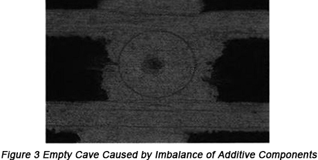
It's quite important to control components and amount of additives and the failure of component control leads to bad copper filling of blind vias or empty cave, as is shown in Figure 3.

The resolution to the failure of empty cave caused by this reason lies in the control in terms of additive components and additive amount, including:
a. Additive flow amount should be periodically calibrated to ensure accurate flow amount so that effective control can be obtained.
b. Carbon treatment should be periodically carried out to solution based on the condition of plating solution pollution.
c. Agent components are analyzed periodically and additive content and plating effect should be estimated by Hull Cell experiment to verify whether the plating effect is within the normal category and corresponding adjustment has to be made in time.
• Cause of foreign matter
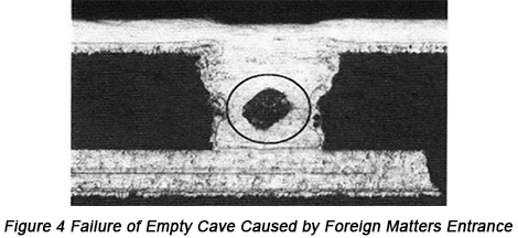
The environment of copper filling plating procedure lines, applied supplies and daily production activities will all lead to pollutions with different pollution degrees. All kinds of foreign matters or contaminants are inevitable. For micro foreign matters, they can't be seen by our eyes and it's extremely difficult to eliminate them. Once they enter blind vias, empty cave tends to be made, as is shown in Figure 4 below.

For this empty cave failure in blind vias, the cause for it is easy to be found. Through SEM, the shape of empty cave in blind vias can be observed. Therefore, the measures to find out source of foreign matters include:
a. External foreign matters are prevented from entering plating solution and enclosed procedure line is suggested.
b. Estimate whether applied materials or agent purity reaches the standard and whether it meets the requirement of PCB manufacturing.
c. Periodic filtering and purity should be implemented on plating agent to ensure the vividness and clear color.
Conclusion
Naturally, the causes for empty cave failure in blind vias are far more than listed and there are a lot of causes for that including material classification of dielectric constant, thickness, blind via type and current parameters of electric plating.
In conclusion, the key is to find out the reason for empty cave failure in blind vias confronted with empty via failure. Meanwhile, it's a good idea to observe empty cave failure shape and summarize experience, to find concerning rules and to implement research with all kinds of analysis methods. Furthermore, based on the mechanism of empty cave failure, scientific operation guidelines should be enacted and improvement and prevention rules should be strictly carried out so that problems can be solved to constantly increase the yield and reliability of products.
Helpful Resources
• Introduction on Blind Via
• 3 Important Elements You Don't Know about Buried and Blind Via in HDI Flex-rigid PCBs
• An Introduction of a New Blind-hole Filling Method: Panel-Plating Blind-Hole Filling
• How to Design Blind/Buried Vias in High-Speed Digital Circuits
• Full Feature PCB Manufacturing Service from PCBCart - Multiple Value-added options
• Advanced PCB Assembly Service from PCBCart - Start from 1 piece
