As chip components and SMT (surface mount technology) are massively accepted by electronics industry, traditional PCBs (printed circuit boards) with organic laminates as substrate material are developing towards high precision, high density and high reliability. As a relatively new type of circuit boards, Ceramic PCBs have received tremendous attention from the industry since they have been regarded as an effective solution for miniaturization achievement of modern electronic products and electronic assembly technology. Thus, this article will provide a comprehensive introduction of ceramic PCBs in terms of their characteristics, categories, fabrication method and applications.
• For Implementation of Miniaturized Electronic Products
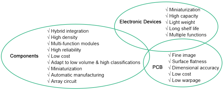
Up to now, human society is moving towards an information society and available information and data that are ready to be processed so electronic devices is urgent to be miniaturized such as telecommunication devices, computers and automatic control equipment. In the past 10 years, miniaturization was achieved primarily by the application of semiconductor chip micro-fabrication technology. Up to now, both LSI (large-scale integration) and VLSI (very large-scale integration) have been making constant progress towards high integration, large scale and high speed and the application of micro-fabrication technology is still an initial solution for electronics miniaturization. After all, when it comes to electronic devices or systems, apart from multiple LSI and passive components, circuit functions won't be implemented unless tracing is carried out for connection. Therefore, how to assemble the maximum number of components on the surface of minimum circuit board is another concern for electronics assembly. Current relationship between market demands, components and PCB can be summarized in the following figure.
• Challenge Confronted by Traditional PCB
Fabricated in substractive process, traditional PCBs with organic laminates like epoxy, polystyrene and polytetrafluoroethylene as substrate material have been applied to participate in circuit assembly as early as latter half of 1950s. Even on the day when VLSI is widely applied, they are still applied to large extent. However, with the advent of SMT and constantly improving of semiconductor circuit integration, traditional PCBs have to face up with the following challenges when they are used in high-reliability electronic products.
a. Heat Dissipation Challenge
Along with increasingly wider application of VLSI and SMT development trend, organic laminated based PCBs are quite challenged by heat dissipation in terms of design, which results from low thermal conductivity of most ordinary PCBs. Nevertheless, ceramic features thermal conductivity that is 90 times of that of epoxy glass fiber, leading to excellent conduction cooling. Moreover, components on ceramic PCBs usually feature a lower junction temperature (Tj) than that on ordinary PCBs.
b. CTE Compatibility Challenge
SMT that became popular in the early half phase of 1980s is affecting the whole electronic assembly industry. Since SMT makes electronic components directly soldered onto both sides of PCB, compared with THT (through hole technology), SMT leads to lower cost and higher reliability. Furthermore, it makes it more accessible to implement automation and capable of reducing circuit size by five sixths.
Some reliable packages, LCC (leadless chip carrier) for example, are so compatible with SMT requirement but they usually fail to withstand challenges brought by thermal cycle. As a result, LCC is doubted from the perspective of packaging reliability to interconnection on board, which is because CTE (coefficient of thermal expansion) incompatibility between LCC and PCB material leads to soldering failure. Therefore, ceramic PCBs come into being. Ceramic PCBs are capable of providing optimal solutions for defeating thermal cycle failure because they share compatible CTE with leadless ceramic chip carrier and feature higher thermal conductivity, higher stability and inertia.
Properties of Ceramic PCB
Compared with traditional PCBs whose substrate materials are epoxy glass fiber, polyimide, polystyrene and phenolic resin, ceramic PCBs feature the following properties:
• Excellent thermal conductivity
• Chemical erosion resistant
• Agreeable mechanical intensity
• Compatible with CTE of components
• Easy to implement high-density tracing.
Due to increasingly multiple functions, miniaturization and high speed of electronic devices and upsizing of IC, more rigorous requirement has to be set to ceramic PCBs in terms of CTE, thermal conductivity, loss, dielectric constant and tape resistance. It can be estimated that ceramic PCBs will be increasingly more called for with aluminum nitride, mullite and glass ceramic as substrate material.
Classifications of Ceramic PCB
In accordance with ceramic PCB fabrication methods, they can be classified into three categories: high-temperature co-fired ceramic PCB, low-temperature co-fired ceramic PCB and thick film ceramic PCB.
• High-Temperature Co-fired Ceramic (HTCC) PCB
As a traditional manufacturing method, high-temperature co-firing is achieved through mixing aluminum oxide and adhesive, plasticizer, lubricant and solvent, leading to raw ceramics by roll forming and curtain coating and implementing circuit tracing on refractory metals like tungsten and molybdenum. Then, it will enter high-temperature oven under 1600°C to 1700°C temperature and carry out baking for 32 to 48 hours after cutting and lamination. To stop tungsten and molybdenum from being oxidized in high temperature, baking should be done in reducing gas such as hydrogen or mixed gas.
Ceramic PCBs manufactured by high-temperature co-firing can be applied on small-scale boards, derived boards or carrier circuits. When it comes to large-scale boards, however, high-temperature co-fired ceramic PCBs are challenged due to their unsuitable shrinking tolerance, warpage and relatively high tracing resistance of refractory metals.
• Low-Temperature Co-fired Ceramic (LTCC) PCB
Low-temperature co-fired ceramic PCB is fabricated by mixing crystal glass, glass composite and non-glass with adhesive with sheet generated and circuit tracing will be implemented by gold paste with high conductivity. After being cut and accurately being formed, it will be placed into oxidizing gas oven at a temperature of 900°C for baking. Low-temperature co-fired ceramic PCB provides a pathway to precious metal paste for circuit tracing and PCB baking can be completed as long as slight improvement is made to thick film baking. Product precision and shrinking tolerance can be improved as well and further optimizations need to be implemented on mechanical intensity and thermal conductivity.
• Thick Film Ceramic PCB
Thick film gold paste and dielectric paste is repeatedly and alternately printed on ceramic base and goes through baking at a temperature below 1000°C. Although this type of fabrication technology is optimal to large-scale ceramic PCB manufacturing and features relatively high assembly base number, its application is limited due to high cost of gold that also stops solder paste from precipitation. As a result, multi-layer thick film copper circuit technology is developed, which is the most noticeable and popular ceramic PCBs. To prohibit copper from being oxidized, this type of ceramic PCB has to be baked in nitrogen gas, which is the key point of this technology. Furthermore, dielectric paste is generated in nitrogen gas depending on complex multi-layer interconnection structures, which is also a core technology.
Application Fields of Ceramic PCB
Ceramic PCBs are widely applied owing to their high thermal conductivity, low CTE, chemical erosion resistance and low dielectric constant.
• Memory Module
AGC company from Japan created 1Mbit SRAM memory module by taking advantage of multi-layer ceramic PCB containing 4 IC chips, contributing to high reliability and high density assembly. Vitarel company from the US created missile, telecommunication products and aerospace products with ceramic PCBs. The common feature all of them are sharing lies in the fact that they can be applied in extreme environment. At warhead, multi-layer ceramic PCB and packaging components on it perform sufficient intensity and shock vibration resistance capability.
• Receiving/Transmission Module
Westinghouse company from the US produced receiving/transmission module for radar with ceramic PCB. Aluminum nitride features high thermal conductivity and low CTE, laying solid foundation for the application of ceramic PCBs in receiving/transmission module.
• Multi-layer Interconnect Board
To be compatible with miniaturization of electronic products, ceramic PCBs are able to hold more components within the same board area, which adds more possibilities for ceramic PCBs in the applications of multi-layer interconnect board.
• Analog/Digital PCB
AGC company from Japan took advantage of LTCC PCBs to produce analog/digital PCB boards so that parasitic capacitance can be reduced by approximately nine tenths. It not only effectively overcomes crosstalk interference of circuit tracing, but also reduces volume and weight of circuit.
All in all, ceramic PCBs have wide application fields due to high thermal conductivity, low CTE and low dielectric constant. They will definitely play a significant role in application fields calling for high reliability, high air sealing and high thermal conductivity. You may reach our sales team on this page for FREE ceramis pcb fabrication quote.
Request Your CustomCeramic PCB Quote from PCBCart Now
Helpful Resources
• Printed Circuit Boards Introduction and Categories
• PCB Material Selection Guide
• PCBCart Offers Full Feature PCB Fabrication Service
• Advanced PCB Assembly Service from PCBCart


