Flex-rigid PCB combines properties of both flexible PCB and rigid PCB, providing a new connection method between electronic devices and parts. Flex-rigid PCB works especially suitable for portable electronic products and wearables, meeting the demands of current market due to its small number of connection points and its capability to improve products' performance.
In spite of its obvious merits, flex-rigid PCB has to be confronted with some difficulties in fabrication process including high complexity of manufacturing technology, numerous process phases, long manufacturing cycle, and high manufacturing cost. Therefore, this article will provide a summary based on which protruding issues will be discussed in terms of engineering source design and fabrication process.
• Structure of Flex-Rigid PCB
Flex-rigid PCB is produced by bonding rigid outer with flexible PCB and circuits belonging to rigid part are interconnected with those to flex part through plated via. Each piece of flex-rigid PCB board contains one or more rigid board parts and flexible board parts. Thus, flex-rigid PCB features multiple structures calling for different fabrication technologies.
• Process Design of Flex-Rigid PCB
a. When it comes to fabrication process of flex-rigid PCB, more attention should be paid to new phases that aren't held by traditional rigid PCB: flex circuit board fabrication (covering material cutting, graphics generation, cover film lamination and punching), low-flow PP (prepreg) window, Plasma cleaning, Plasma roughening, pre-milling, laser cutting, shielding film lamination, stiffening board lamination.
b. Equivalent with rigid PCBs, flex-rigid PCB design should be implemented by professional PCB design software that is selected based on designer's preference and board requirement.
• Layout Design of Flex-Rigid PCB
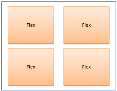
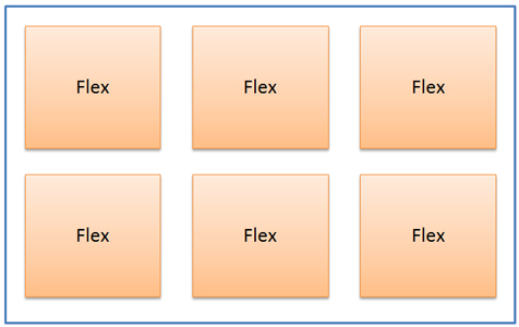
Flexible copper clad laminate (CCL) is usually designed to feature two selections of widths: 250mm and 500mm. Generally speaking, flexible PCB features a size range from 250mm×100mm to 250mm×250mm while rigid PCB features a size range from 18in×24in to 21in×24in. When it comes to flex-rigid PCB, therefore, layer up technology is demanded with leading structures demonstrated as the following.
a. Four pieces of flexible boards are combined to be a large board whose size is the same as that of rigid boards.

b. Six pieces of flexible boards are combine to be a large board whose size is the same as that of rigid board.

• Low-Flow Prepreg
a. The thickness range of ordinary no-flow PP is from 40μm to 125μm and core board thickness of ordinary rigid board is at least 3mil while the thickness of ordinary one-layer flexible board is 0.5mil. Compensation standard of low-flow PP regulates adhesive overflow of 0.7mm as a critical point. When customers require overflow adhesive volume to be more than 0.7mm, 5mil should be compensated towards flexible area along De-Cap line in customer's design file. When customers require overflow adhesive volume to be less than 0.7mm, it should be indicated in NPI (new product introduction).
b. The alignment between low-flow PP and core board is achieved through the application of OPE machine for punching and alignment. OPE hole is punched after core board is fabricated and corresponding holes are drilled at corresponding positions on low-flow PP.
c. Alignment acceptance criteria is less than 4mil. Copper aperture should be seen with decuple magnifier and PP can't be seen within the aperture, which means that PP can be only tangent with PP. As is depicted in the previous part of this article, four in one or six in one lamination type is applied. Flexible board and rigid board are fixed through rivets so rivet holes should be drilled in advance on low-flow PP corresponding area. Hole diameter and hole positions are equivalent to those of rigid boards, that is, each piece of flexible board calls for four rivet holes. When it comes to six in one board, PP will demand 24 rivet holes.
• Plasma Cleaning and Roughening
Flexible board covered with Coverlay needs Plasma cleaning prior to lamination with cleaning conditions#1 conformed to. As far as the whole board covered with Coverlay is concerned, Plasma roughening is added before lamination with cleaning conditions#2 conformed to. Cleaning condition#1 and condition#2 can be summarized into the following table.
|
Item
|
Condition 1
|
Condition 2
|
| RF (KW) |
2200 |
2200 |
| Time (min) |
5 |
8 |
| Temperature (OF) |
180 |
180 |
| CF4 (cc/min) |
600 |
600 |
| O2 (cc/min) |
1300 |
1300 |
• Riveting Jig Manufacturing
As flexible board and rigid board need riveting with rivets, it's quite difficult to carry out manual riveting, which therefore demands riveting jig. The parameter of dowel on riveting jig is smaller than that of riveting jig by 25μm. From the length of board, rivets are arranged in four rows and dowel is placed at two rows of rivets on rivet jig.
• Solder Mask Technology Selection and Design Requirement
a. As far as flex-rigid PCB is concerned, when its thickness is more than 0.5mm, spraying coating can be applied and thin board usually takes advantage of silkscreen technology.
b. Solder mask window opening on flexible board should be more than 4mil to 8mil from board axle wire towards rigid area.
c. When it comes to flex-rigid PCB applying De-Cap technology, block light points and solder mask window opening shouldn't be implemented on De-Cap area. When De-Cap design isn't available, silkscreen should be designed to block light.
• Pattern Milling Design
During the process of flex-rigid PCB fabrication process, flexible materials need to be laminated with rigid materials and surface rigid materials will be eliminated through a special method in order to make flex board at specific area exposed. Then, surface finish will be implemented on the area with flexible board exposed and the complete pattern will be milled out. As a result, a flex-rigid PCB will be finally generated.
• De-Cap Design
De-Cap alignment target design is actually conformal mask alignment holes after lamination. Target at flexible area should not be selected for De-Cap. If the design requires that flexible target alignment is demanded to be used, diameter of this target image should be 0.4mm at most. Furthermore, each plane should make use of its own fiducial marks.
• Flex-Rigid PCB Strengthening Design
Connection parts on flex-rigid PCB should be designed to be on flexible board. Moreover, copper should be coated at the connection part without copper exposed to the air. As a result, flexible part and rigid part will not be separated.
• Strengthening and Shield Film Design
Strengthening board aims to strengthen the rigidity of flexible boards. Shield film manufacturing conforms to customers' design file.
Flex-rigid PCB design features complex structures and leads to difficult design and manufacturing technology. Furthermore, flex-rigid PCB calls for numerous types of materials with a high cost. Flex-rigid PCB fabrication witnesses accuracy control as a key point, leading to high demand in terms of dimensional stability. What has been discussed in this article is expected to be able to provide a reference for engineers to optimize flex-rigid PCB designs, which thereafter guarantees the reliability and performance of electronic products.


