EMC, short for Electro-Magnetic Compatibility, refers to a coexistence state in which electronic devices are capable of implementing their own functions in the same electromagnetic environment. Put it simply, EMC allows electronic devices to work independently and normally with no interference between them, that is, those electronic devices can be compatible with each other in the whole system. Because EMC is achieved by controlling EMI (Electro-Magnetic Interference), it develops with a series of studies concerning EMI such as introduction of EMI, research on EMI, anti-EMI solutions and EMI management.
Fundamental Principles of EMC
To reduce interference between digital signals and analog signals, you need to know two fundamental principles of EMC first.
Principle 1: Circuit loop area should be MINIMIZED.
Principle 2: Only a SINGLE reference plane can be applied in a system.
Once Principle 1 fails to be followed and signals have to pass a large loop area, a large loop antenna will be generated. However, once Principle 2 fails to be followed and two reference planes are available, a dipole antenna will be created. Neither of the results is what is expected.
Mix-Signal PCB Partitioning Rules and Applications
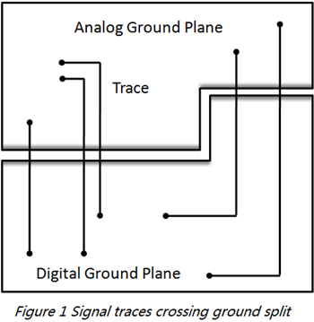
It is advised that digital ground and analog ground on the same mix-signal board should be separated so as to achieve isolation between them. In spite of the feasibility of this solution, lots of latent issues will occur, which are protruding especially in large-scale systems. The crucial problem lies in the fact that tracing fails to be set up across the split between digital ground and analog ground. With tracing set up across the split, both electromagnetic radiation and signal crosstalk will drastically rise. The most commonly seen issue in PCB design lies in EMI occurrence due to signal lines crossing split ground or power.
Figure 1 below depicts the situation introduced above.

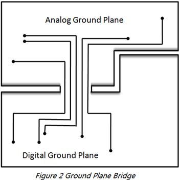
Based on this split method, signal lines have to go across the split between digital ground and analog ground. Then, what does signal circuit return path look like? Suppose that two split grounds are connected together at one point and under this situation, a large loop will be generated by ground circuit. Thereafter, high-frequency circuit flowing across large loop will lead to the occurrence of a large loop with high ground capacitance and radiation generated. If low level analog circuit flows across the large loop, it will be easily interfered by external signals. The worst situation will take place when split ground is connected with power, an extremely large circuit loop will be formed. Furthermore, a dipole antenna will be formed when analog ground and digital ground are connected together through a long lead. As a result, engineers should know the path and method of return circuit in mix-signal PCB design optimization. However, many engineers look upon the flowing path of signal circuit without thinking about circuits' specific path. If ground plane has to be split and tracing has to be arranged across the split, single point connection can be first implemented between two split grounds with bridge formed so that a direct current return path will be provided under each signal line with a small loop area formed, which is indicated in Figure 2.

Application of optical isolation devices or transformers also can lead signals across split. When it comes to optical isolation devices, it is optical signals that go across split. When it comes to transformers, it is magnetic field that goes across the split. Another applicable method lies in the application of differential signals. Signal flows into a line while returning from another signal line. Under this condition, ground is not required as a return path.
Split partitioning can be applied in the following three circumstances:
Circumstance 1: Some medical equipment requires a low leakage current between circuit connected with patients and system.
Circumstance 2: Input from some industrial process control equipment may be connected with electromechanical devices with high noise and power.
Circumstance 3: PCB layout suffers from certain limitations.
Independent digital and analog powers are usually available on mix-signal PCBs and split power planes can and should be depended. However, signal lines closely ambient to power planes fail to go across the split between powers and all signal lines crossing this split have to be ambient to conductor planes with large area. In some situations, split issues concerning power planes can be avoided through designing analog power to be PCB connecting wires instead of just a plane.
Ground Plane Layout Method and Applications of Mix-Signal PCB
To discuss the interference left by digital signals on analog signals, attributes of high-frequency current have to be understood first. High-frequency current always depends on the path with minimum impedance (lowest inductance) and directly lies under signals. As a result, return path will flow across ambient circuit plane no matter this plane is power plane or ground plane. In practical operation, ground plane tends to be used with circuit board partitioned into analog section and digital section. Analog signals are laid within analog sections of all planes while digital signals within digital circuit area. In this situation, digital signal return current won't flow into the ground of analog signals. As long as digital signal layout is carried out above analog section or analog signal layout is carried out above digital section in PCBs, interference produced by digital signals on analog signals will be generated.
The occurrence of such issues doesn't derive from absence of split ground but the unsuitable layout of digital signals. When it comes to PCB design, ground plane application, partitioning by digital circuits and analog circuits and reasonable signal layout usually help solving difficult problems concerning layout and partitioning. Moreover, some potential problems caused by split ground can be avoided. As a result, component layout and partitioning become key elements determining the quality of PCB design. If layout and partitioning are suitable enough, current in digital ground will be limited in digital section in a circuit board with analog signals stopped from being interfered. Layout for such situation has to be carefully inspected and checked to ensure layout rules have to be totally conformed to. Otherwise, even an unsuitable signal line layout will possibly lead to the breakdown of a whole circuit board.
When analog ground and digital ground pins of A/D converter are connected together, most A/D converter manufacturers will suggest connect ADND and DGND pins with the same ground with low impedance through minimum leads. That's because those pins are not connected inside most A/D converter IC and any external impedance connected with DGND will lead more digital noise coupled with analog circuit inside IC through parasitic capacitance. Accordingly, both AGND and DGND pins of A/D converter should be connected with analog ground. Nevertheless, it will arouse an issue that whether analog ground or digital ground should be connected with grounding terminal of decoupling capacitor of digital signals.
When it comes to the system with a single A/D converter, the issue introduced above can be easily solved. With ground separated, analog ground section and digital ground section are connected under A/D converter. When this method is being used, bridge between two grounds should be as wide as that of IC and any signal line shouldn't go across split.
When it comes to a system with a few A/D converters, 10 for example, how should we connect? If we follow the same solution as introduced above, that is, to connect analog ground and digital ground under A/D converter, multiple point connection will be caused so that isolation between analog ground and digital ground will become meaningless. If the connection isn't carried out like this, manufacturer's requirement won't be met. The optimal solution lies in the application of uniform ground that is divided into analog section and digital section. This type of layout not only meets the requirement on analog ground and digital ground from IC manufacturers who demand low impedance between them but avoid issues against EMC such as loop antenna or dipole antenna.
If engineers hold doubt on uniform ground application in PCB design, layout can be implemented based on ground plane split method. In the process of design, board should be accessible to jump wire with less than 0.5inch or 0ohm resistor to connect split ground. Much attention should be paid to partitioning and layout in order to ensure no digital signal lines are placed above analog section and vice versa. Furthermore, any signal line mustn't go across ground split or split isolating powers. To test functions of PCB and its EMC, two grounds should be connected through 0ohm resistor or jump wire and then retest functions of the board and its EMC. Result comparison indicates that in all cases, uniform ground solution is better than split ground solution in terms of functions and EMC.
Mix-signal PCB design is a complicated process. A PCB should be partitioned into independent analog section and digital section and A/D converter should be placed across sections. To separate analog and digital powers, split between isolated power planes shouldn't be crossed and signal lines that have to be crossed should be arranged at the circuit layer that is ambient to large area. Where return path current flows and how it flows should be analyzed so that suitable component layout and correct layout rules should be conformed to. In all layers of a circuit board, digital signals can only be laid out in digital sections whereas analog signals can only be laid out in analog sections.
Ground Plane Layout Method and Applications of Mix-Signal PCB
If you ever completed a pcb design and need someone to help bring it into real circuit board. Please feel free to reach us for solution. We've over two decades' experience in custom PCB manufacturing. We've all it takes to fabricate your PCBs with all the functions you demands quickly and cost-effectively.
Electro-Magnetic Compatibility (EMC) enables electronic devices to coexist in synchronization without interference, critical in mixed-signal PCB design. With the application of methods such as shrinking the areas of circuit loops and employing single reference planes, engineers can effectively minimize unwanted electromagnetic effects. Effective partitioning of analog and digital sections and effective ground plane designs isolate crosstalk and noise interference, enhancing signal integrity and system performance.
If you have a completed PCB design and need expert assistance to bring it to life, PCBCart is here for you. With over two decades of manufacturing custom PCBs, we have the skills and expertise to have your PCBs produced quickly and affordably. We stand behind quality and precision to make sure your boards will meet all your functional requirements, delivering stable performance. Contact PCBCart today and experience a smooth transition from design to production.
Get a Quick and Free PCB Layout & Design Quote from PCBCart
Helpful Resources
• The Most Comprehensive Introduction of EMI and EMC Automated Tools
• Ensuring First-Time Success in PCB EMC Design
• PCB Layout Influence of Electronic Product EMC Performance
• Problems of EMC Technology Application in PCB Design of Electronic Devices and the Strategies


