The most basic form of design for manufacture as it applies to PCBs is the use design rules and design rule checking in PCB design software. Design rule checking (DRC) is the process of looking at a design to see if it conforms to the manufacturing capabilities of a PCB fabricator. Typically the designer will get the highest tolerances that a PCB fabricator supports from the fabricator, load these tolerances into their design program and then run a design rule test on their prospective design. Design rule checks are commonly integrated into PCB design software and are not typically considered as add on service. More advanced design for manufacture analysis software is also available to look for more complex and less obvious design flaws. Typically, DFM software checking is offered by PCB fabricators to customers as an extra service. The reason for this distinction is because of the plus cost of high end DFM software and the additional training required for using it.
1. Starved thermals
Starved thermals occur when the thermal relief traces connected to a pad are not properly connected to the associated copper plane. Quite often, the spacing between vias will pass a basic design rule check, but the attached thermal relief traces will be interrupted and the effected vias will be inappropriately isolated from their assigned copper pours. This issue is most commonly seen when multiple vias are placed in proximity to each other.
2. Acid traps
When two traces are joined at a highly acute angle it is possible that the etching solution used to remove copper from the blank board will get "trapped" at these junctions. This trap is commonly referred to as an acid trap. Acid traps can cause traces to become disconnected from their assigned nets and leave these traces open circuited. The issue of Acid traps has been reduced in recent years by fabricators switching to the use of photo activated etching solutions. So, while it is still a good idea to make sure that your traces do not meet acute angles, the issue is less of a worry than it had been in the past.
3. Silvers
If very small portions of a copper pour are only connected to larger portions of the same copper pour through a narrow trace, it is possible for them to break off during fabrication, "float" to other parts of the board and cause unintended shorts. The problems presented by silvers have been reduced in recent years by fabricators switching to the use of photo activated etching solutions. So while silvers are still to be avoided in designs, they are not as predominate of an issue as in the past.
4. Insufficient annular ring
Vias are made by drilling through pads on either side of a board and plating the walls of these holes to connect the two sides of the board. If the pad size called out in the design is too small, the via may fail due to the drill hole taking up too large of a portion of the pads. Minimum annular ring size is commonly part of the DRC process. This issue is mentioned here because of the not uncommon occurrence of missed drill hits in prototyping boards.
5. Via in Pads
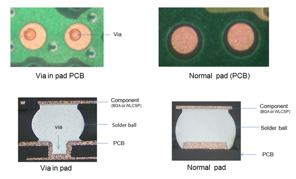
Occasionally it may be convenient to design via to be positioned within a PCB pad. However, via in pads can cause issues when the time comes for the board to be assembled. Via will draw solder away from the pad and cause the component associated with the pad to be improperly mounted.
The image below shows difference between via in pad PCB and normal PCB.
6. Copper too close to board edge
Normally caught during design rule checks, placing copper layers too close to the edge of a board can cause those layers to short together when the board is cut to size during the fabrication process. While this sort of error should be caught using DRC features typically available in PCB design software, a PCB fabricator that does a DFM check will also catch this issue.
7. Missing solder mask between pads
In very tightly spaced, small pin pitch devices, it is quite common for there to be no solder mask between pins due to standard design settings. The omission of said solder mask can lead to solder bridges forming more easily when the fine pin pitched component is attached to the PCB during assembly.
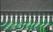
We has been providing professional PCB assembly services for years, we are capable to refrain from missing solder mask between pads. The image below shows our high precise solder mask between 0.4 pitch QFN pads.
8. Tombstoning
When small passive surface mount components are soldered to a PCB assembly using a reflow process, it is common for them to lift up on one end and "tomb stone". Tombstoning can greatly affect PCB yields and quickly drive up production costs. The source of tombstoning can be incorrect landing patters and imbalanced thermal relief to the pads of the device. Tombstoning can be effectively mitigated by the use of DFM checks.
Below image is a tombstoning sample and its schematic.
Have PCB Design file in Hands? PCBCart Can Take Care of Your PCB Fabrication!


