With power components coming in smaller and smaller surface mount packages it is important to come up with a coherent approach to mitigating the thermal dissipation demands of these components in a PCB design. While the development of an exact mathematical analysis of the thermal characteristics of a PCB design can be a complex process, it's possible to apply some simple rules to improve the thermal conduction of your design. Ultimately, properly controlling the dissipation of heat in your design will allow you to produce a more reliable and economical PCB design. What follows is a brief discussion of the standard thermal dissipation model and then some general rules for dealing with thermal dissipation in your designs.
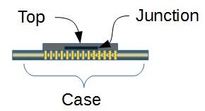
First it is important to define the terminology that is going to be used through the rest of this entry. The next figure presents the different components to a power IC that we must consider when discussing thermal management. We will be discussing the temperature of the Junction, Top and Case of the component and their thermal resistances to the ambient environment throughout this article.

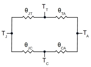
With these terms in hand, we will briefly look at the standard model used to simulate the thermal dissipation of a component. Thermal resistance is normally modeled as a resistor network. The standard model for a component is presented in the following figure:

In the presented figure TJ is defined as the temperature of the junction (the internal working portion of the component), TT is the temperature of the "top" of the package (typically the plastic enclosure of the component), TC is the temperature of the "case" (this is the temperature of the highly thermally conductive pads of the component and the attached PCB) and TA is ambient environment's temperature. The goal of the electronics designer is to then produce the lowest thermal resistance possible between the junction and the ambient environment. With the exception of θCA, the thermal resistances of the system (θJT, θTA and θJC) are defined by the properties of the component and can be pulled from the data sheet for said component. As a PCB designer we principally have influence over the value of θCA, which is dependent on our PCB design. As such, the primary challenge for the designer is the reduction of the thermal resistance of the IC's case to the ambient environment by reducing this resistance. How well we are able to lower this thermal resistance (θCA) will largely define the temperature differential (or lack thereof) that will develop between the ambient environment and the junction of the component.
Of note is that the other path for thermal conduction is the plastic case (or the "top") of the component. As the plastic packaging of most power components do not provide a good thermal path to the ambient environment the efficiency of thermal dissipation of the design is more heavily dependent on the design's ability to dissipate thermal energy to the surrounding environment through its case. The only exception is when the power IC in question is designed with a thermal pad located on the top of the component. In this case, the IC is designed for a heat sink to be attached directly to the top of the IC and the thermal dissipation of the component through its "top" becomes a much more important factor in the design.
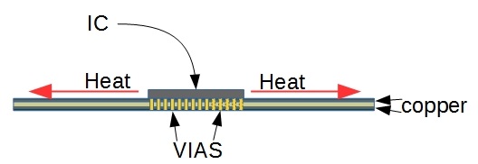
The standard approach to translating heat away from power components is through thermally connecting the power components to adjacent copper planes by way of thermal vias. This is typically achieved by placing a number of vias in the foot print of the power IC. These vias provide a thermal connection to the copper layers below the IC, which then conduct heat away from the component.

Additionally, the more power copper planes connected to power IC by said thermal vias, the higher efficiency of thermal dissipation of the PCB. e.g. using a 4-layer design vs. a 2-layer design can increase power dissipation capacity of the PCB up to 30% when comparing the same area of those designs.
The following design rules are provided as a good starting point for approaching the thermal considerations of your design.
a. In order to dissipate 1 watt of power a good rule of thumb is that your board with need to have an area of 15.3 cm² or 2.4 in² per watt dissipated for a 40°C rise in board temperature. If the board is subject to airflow this requirement can be cut in half (7.7 cm² or 1.2 in² per watt). These values assume that the component is thermally coupled to a copper plane that extends to the edges of the board and that the board is positioned so that air can flow freely around both sides of the board. If these power density requirements are too constrictive for your design, the inclusion of an external heat sink may be required. Also, a 40°C temperature rise is a good starting point to consider when controlling your circuit board's temperature.
b. Whenever there is more than one power component being placed on a board, it is best practice to place those components in such a way that your PCB is being evenly heated by these components. Big temperature differences across the length of you PCB design do not allow your PCB to optimally translate thermal energy away from the mounted power components. If available to the designer, thermal imaging can allow for the empirical inspection of your component placement once a design revision is complete.
c. The more vias that you can place below your component the better your PCB will translate thermal energy to the connected copper plane. Array vias to increase the number in contact with the power pads of your package (the large thermally conductive pads of the component).
d. In designs that dissipate higher wattages you will need to use higher copper weights. 1oz copper is recommended as a starting point for power designs.
e. When utilizing a copper pour to dissipate thermal energy away from a component, it is important that the pour not be interrupted by tracks that run perpendicular to the thermal path away from the power component.
f. If a heat sink needs to be utilized to keep the temperature of the system in tolerance it is of note that the heat sink will typically be much more effective if placed in such a way that it is thermally connected to the case of the component. This typically means attaching the heat sink to the opposite side of the board from a surface mounted component. While it may be tempting to place a heat sink directly on the top of the component, the thermal resistance of the components plastic case will render the heat sink in-effective. As noted above, the exceptions to this rule are packages explicitly designed to have heat sinks attached to their "tops".
In summary, the thermal performance of a design is very important to consider whenever you are working with power components. Using the design rules presented in this article early in the design process of your PCB will allow you to get a good head start on controlling the temperature of your PCB and allow you to avoid drastic redesigns later in the development process.
In general, thermal performance of PCB design should be done accurately, especially while designing with tiny power component packages. Thermal dissipation should be addressed early enough in the design phase to guarantee the cost efficiency and reliability of the final product. By executing key methods such as thermal vias, copper planes, and careful component placement, designers are able to significantly reduce thermal resistance and improve heat dissipation. Following these hands-on guidelines can lead to an optimized design that avoids overheating risk and extends electronic component life. For those who are willing to implement these thermal management strategies on their projects, PCBCart provides all-in-one PCB Assembly and Manufacturing services. With quality and accuracy as our priorities, PCBCart is capable of making your designs a reality, with solid and efficient solutions. Receive a quote from PCBCart today and begin creating your innovative PCB designs with expert industry-leading support.
Get an Instant Quote for PCB Assembly & PCB Manufacturing
Helpful Resources
• The Most Comprehensive Principles of Thermal Design for PCBs
• Internal Thermal Dissipation Design of PCB based on Thermal Model
• Tips of Thermal Design for PCBs Controlled by FPGA System
• Design of High-Power PCB in High Temperature Environment
• Metal Core PCB an Ideal Solution to Thermal Issues in PCB and PCBA
• Full Feature PCB Manufacturing Service from PCBCart - Multiple Value-added options
• Advanced PCB Assembly Service from PCBCart - Start from 1 piece
