



Three decisions set how a Rogers board behaves in fabrication and assembly: the laminate you pick, how you build the stack-up, and which surface finish goes on the pads. Pick the laminate for the Dk your design needs and the Dk tolerance you can live with. Keep the stack-up pure Rogers and give us the dielectric thickness your impedance model assumes. Choose from ENIG, immersion silver, immersion tin or OSP, because HASL is not offered on these boards.
The sections below go through each decision as we see it from the fabrication side.
Which Rogers laminate fits which job?
Start from the Dk your circuit needs, then look at how tightly that Dk is controlled. The image below shows the laminate we reference for high-frequency boards, with Dk measured at 10 GHz:
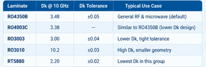
RO4350B is where most RF projects begin, and for good reason. It is the most common request we see, and the Dk tolerance is tight enough that it rarely drives the impedance error. If your simulation was done on RO4003C, do not swap to RO4350B to "save a step". The 0.10 difference in Dk shifts your line widths, and you would be re-running the model anyway.
RO3010 is the outlier. A Dk of 10.2 gives narrow lines and small structures, which is the point, but it also means your etch tolerance matters more because everything is smaller. RT5880 and RO3003 behave differently from the RO4000 family during drilling and handling, so if your design uses them, tell us early. The specifics of process settings for each laminate are something to confirm with our engineering team before you commit the layout.
Our PCB materials page lists the broader material range, but for RF work the table above is the practical shortlist.
What should you specify in the stack-up?
We build Rogers boards from 2 to 24 layers, with finished thickness from 0.4 to 5.0 mm and finished copper from 0.5 to 2 oz. Within that window, a few things keep the stack-up buildable and the impedance predictable.
Keep the construction pure Rogers. Every core and every bonding layer comes from the Rogers family, and the prepreg set includes Rogers 4450F. Mixing laminate families in one stack adds lamination and registration questions that are outside what we are describing here, so this article does not cover it. If your design needs something different, send it over and we will review it separately.
Build the stack-up symmetrically around the center. An asymmetric build on a thin board is the most common reason we see warp complaints, and it is also the cheapest thing to fix on paper before the order is placed.
State the dielectric thicknesses your impedance calculation used, not only the total board thickness. A 1.6 mm finished board can be built several ways, and your controlled-impedance traces only match your model if the dielectric between the trace and its reference plane matches what you assumed. We will propose a build if you do not have one, but we would rather check yours.
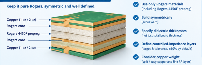
Say which layers carry controlled impedance, and the target and tolerance for each. Our impedance tolerance is ±10%. If your design needs tighter, confirm with our engineering team before finalizing the layout, because it changes how we verify and may change the construction.
Copper weight deserves a quick thought. Heavier copper on an RF signal layer makes fine geometry harder to hold, so if your power section needs 2 oz and your RF section needs fine lines, talk to us about how to split them across layers.
How tight can trace, spacing and impedance be?
Our minimum trace width and spacing is 3/3 mil, with a minimum annular ring of 4 mil and a minimum drilled hole of 6 mil. Impedance tolerance is ±10%.
Those are minimums, and we would not design an RF line to sit on them. Narrow lines on a high-Dk laminate such as RO3010 leave very little room for etch variation, so the finished width drifts further from the drawn width in relative terms. Give the critical RF traces some margin and keep the minimum geometry for the places that genuinely need it, such as fine-pitch pad escapes.
Dk tolerance is worth a sanity check. A ±0.05 swing on RO4350B is small next to a ±10% impedance budget, so in practice etch and dielectric thickness usually dominate the error, not the laminate. If you are chasing impedance accuracy, look at your line width tolerance and your dielectric spacing before you blame the material.
Heavy copper combined with 3/3 mil geometry is not a combination to assume. Check it with our engineering team for your specific copper weight.
For layout practice that sits upstream of all this, our high-speed layout article covers routing decisions that affect how the board is fabricated.
Which surface finishes work on RF boards, and why HASL isn't offered
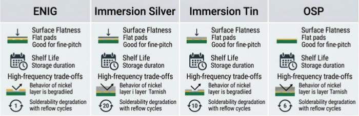
For Rogers boards we offer four finishes: ENIG, immersion silver, immersion tin and OSP. Each has a different trade-off.
ENIG. Flat pads, good for fine-pitch components, and long storage. Some RF designers avoid having a nickel layer under critical transmission lines because of how nickel behaves at high frequency. Others accept it. That is a call for your loss budget, not ours.
Immersion silver. Flat and solderable, and a common pick when the nickel layer is a concern. It needs careful packaging and handling, because silver tarnishes if the boards sit open.
Immersion tin. Flat, with solderability that depends on storage time. Plan your assembly date accordingly.
OSP. Bare copper under a thin organic coating. It is the simplest finish, but the coating degrades with each reflow pass, so it suits boards that see a single assembly cycle.
HASL is not part of our offering for these boards. The surface is uneven, which hurts fine-pitch placement and is a poor match for RF pads where geometry matters. The molten solder dip also puts a thermal shock on the laminate that we would rather not apply to a material you chose carefully for its electrical behavior.
If you are unsure between ENIG and silver, tell us the pad pitch, the number of reflow cycles and how long the boards will sit before assembly. Those three facts usually settle it.
Drilling and handling notes that affect yield
Hole size and annular ring are where Rogers designs most often run into trouble. The minimums are a 6 mil drilled hole and a 4 mil annular ring. On a thick board, a small hole raises the aspect ratio quickly. If you are combining a 5.0 mm build with small vias, confirm the aspect ratio with our engineering team before you route.
PTFE-based laminates need different hole-wall preparation than epoxy-glass, and soft laminates mark easily. We handle these accordingly, but you can help by avoiding unnecessary via counts under RF components and by not placing drilled holes right at the edge of the board outline.
Thin cores are fragile. At 0.4 mm finished thickness the board needs support in handling, and that has an effect on panel design. Ask us about panelization if your board is thin and large.
Specific drilling parameters, bake requirements and storage conditions depend on the laminate. We do not publish them here. Confirm with our engineering team for the material you picked.
Our high frequency PCB fabrication page describes the board types this process covers.
What to send with your RF board order
A complete package saves a round of questions, and on Rogers boards it also saves a round of impedance re-calculation. We usually ask for:
Gerber files, with a drill file and a clear board outline
The laminate name and thickness for every core, and the prepreg you expect
Finished copper weight per layer
The stack-up drawing, with controlled-impedance layers marked and target values stated
Impedance target and tolerance for each controlled net
Surface finish choice from ENIG, immersion silver, immersion tin or OSP
Any via or hole requirement that sits near the minimums (6 mil hole, 4 mil annular ring)
Quality class, if you need something other than our standard IPC Class 2
A note on assembly plans, including the number of reflow cycles, if the boards will be assembled
We work from Gerber files. We do not provide schematic design services, so the electrical design needs to be finished before the package arrives.
FAQ
Can you hold tighter impedance than ±10% on Rogers boards? Our standard tolerance is ±10%. If your design needs tighter, send the stack-up and the target values and confirm with our engineering team. Do not assume it will be accepted just because the laminate Dk tolerance is tight, since etch and dielectric thickness usually move the result more than the Dk does.
The Dk is quoted at 10 GHz. Which Dk should I use in my model? The datasheet values in this article are at 10 GHz. If your design runs elsewhere, ask which Dk we recommend for the model, and confirm the number with our engineering team before you finalize the line widths. We do not state a maximum operating frequency for any laminate here.
Do you build Rogers boards to IPC Class 3? Our standard is IPC Class 2. If your program needs something different, raise it with our engineering team at the quote stage.
Do you help with the RF design itself? No. We fabricate from your Gerber files and do not offer schematic design. We can review the stack-up and fabrication side and tell you where the design is close to a limit.
Can the boards go straight to assembly? Assembly is quoted separately. Tell us at the PCB quote stage that assembly is planned, along with your finish choice and expected reflow cycles, so the finish and the plan agree. Reflow profile details for your specific laminate are something to confirm with our engineering team.
Helpful Resources
• High-Frequency Materials: Rogers vs FR-4
• Impedance Control in PCB
• PCB Surface Finishes Introduction and Comparison
• ENIG vs Immersion Silver: Surface Finish Comparison


