In the process of PCB soldermask manufacturing, the craft of PCB continuous double-side printing liquid soldermask by silkscreen printing nail-bed has been massively applied. Since relatively big differences take place between PCBs in terms of aspects of design including thickness, pattern distribution, via diameter and via distribution, the manufacturing of silkscreen printing nail-bed is extremely difficult. If the distribution of copper nails on nail bed is far from being reasonable, soldermask thickness uniformity is easily caused. The bad result is either the color aberration of soldermask appearance, bad soldermask imaging or solder bridge with broken resistance, leading to rework or scrap. Therefore, detailed instructions have to be established to pertain to nail welding in the process of soldermask silkscreen printing in order to ensure the quality of nail bed.
Theory Analysis
Soldermask with double-side silkscreen printing refers to the process in which liquid soldermask is printed on one side of PCB prior to liquid soldermask printing on the other side using silkscreen printing nail bed. Therefore, continuous printing of soldermask for both sides of PCB can be implemented so that dwell time and heating time can be reduced to improve circuit board manufacturing efficiency.
To manufacture silkscreen printing nail bed, supporting nails should be deployed at the place where the bottom board of nail bed is compatible with PCB board edge or via positions. The complexity of manufacturing process leads to relatively high requirement of technology, so it has to be completed by experienced workers who still possibly suffer from errors in terms of lack of nails welding, low nail distribution density, and position deviation of nail distribution when they are dealing with highly-complicated boards or boards with new type model.
Therefore, it's necessary to analyze the influence on PCB soldermask printing caused by silkscreen nail bed with different nail distribution density so that reasonable nail distribution of soldermask silkscreen printing nail bed regulations can be obtained to increase nail bed manufacturing efficiency and the double-side silkscreen printing quality of soldermask.
Experiment Design
• Experiment factors and horizontal design
For three types of nail distribution density (spacing 5.0cm, 8.0cm, 10.0cm) and PCB thickness (0.8mm, 1.5mm, 2.0mm), experiment is carried out through cross matching and the experiment is designed as Table 1.
|
Test NO.
|
Board NO.
|
Board thickness
|
Nail welding density
|
|
1
|
1#, 2#
|
0.8mm
|
5.0cm
|
|
2
|
3#, 4#
|
8.0cm
|
|
3
|
5#, 6#
|
10.0cm
|
|
4
|
7#, 8#
|
1.5mm
|
5.0cm
|
|
5
|
9#, 10#
|
8.0cm
|
|
6
|
11#, 12#
|
10.0cm
|
|
7
|
13#, 14#
|
2.0mm
|
5.0cm
|
|
8
|
15#, 16#
|
8.0cm
|
|
9
|
17#, 18#
|
10.0cm
|
• Nail bed manufacturing
A bare copper board with the dimension of 457mmx610mm is applied as the nail bed base plate on which copper nails are evenly placed in the mode of array with green transparent tapes fixed. Spacing between copper nails is respectively 5.0cm, 8.0cm and 10.0cm. On the nail bed with different nail distribution spacing, the distance between external nails and the edge of bottom board should be symmetrical vertically and horizontally to ensure that thickness differences won't take place because of the wrong positions of copper nails in the process of silkscreen printing.
Take the spacing of 5cm for example. The length of shorter side of copper board is 45.7cm with 9 nails placed on each row and 2.8cm horizontal clearance while 11 nails are placed on each row along the longer side of the copper board. To sum up, 99 nails are required. Table 2 illustrates the comparison between the number of copper nails and spacing with three selections of copper distribution density.
|
Board size
|
Array size
|
Spacing
|
Amount of nails along short size
|
Amount of nails along long size
|
Total amount of copper nails
|
|
457x610mm
|
40x50cm
|
5.0cm
|
9
|
11
|
99
|
|
40x48cm
|
8.0cm
|
6
|
7
|
42
|
|
40x50cm
|
10.0cm
|
5
|
6
|
30
|
• Test board manufacturing
Bare copper board with the size of 17''x23'' is applied with the thickness of board 0.8mm, 1.5mm and 2.0mm. Each type of boards with different thickness should be provided with 6 pieces and the thickness of copper is 1oz with filet. Take the most commonly-used green liquid soldermask ink as an example. The silkscreen printing parameters are displayed in Table 3 below.
|
Mesh type data
|
43T
|
|
Ink type
|
780H
|
|
Ink viscosity
|
140dPa•s
|
|
Mesh spacing
|
5mm
|
|
Silkscreen printing pressure
|
0.49MPa
|
|
Silkscreen printing speed
|
6Hz
|
|
No. of silkscreen printing knife
|
2
|
• Data accumulation method
Wet film thickness tester is applied for the measurement of thickness of soldermask. Since the test position is along the diagonal line of copper nails, the difference in terms of spacing between copper nails leads to the differences on test array and test point. Take the nail bed with spacing of 5cm for example. The array of wet film thickness for testing is illustrated in Table 4 below.
|
Short side
|
(17x25.4-15)/50=8.36
|
8 copper nails are
acquired at most
|
8x8 copper nails
of array
|
|
Long side
|
(23x25.4-55)/50=10.54
|
10 copper nails are
acquired at most
|
|
|
Number of
test points
|
4x(8-1)+1=29
|
Each board should
have 29 test points
|
|
With the spacing between copper nails to be 5.0cm, only 8x8 copper nails can be acquired, based on which the largest measurable array for other spacing between copper nails and the number of test points can be illustrated in Table 5 below.
|
Spacing
|
Test array size
|
Number of copper nails
on diagonal line
|
Number of
test points
|
Number of
test points
|
Summary number
of points
|
Total number
of points
|
|
5.0cm
|
35x35cm
|
8
|
29
|
58
|
174
|
354
|
|
8.0cm
|
32x32cm
|
5
|
17
|
34
|
102
|
|
|
10.0cm
|
30x30cm
|
4
|
13
|
26
|
78
|
|
In order to obtain the data of dry ink thickness, one nail bed of 5.0cm and one board for each type are prepared. The dry ink thickness data is read within the category of film thickness measurement test. The key experiment data accumulation method is illustrated in Table 6 below.
|
Data type
|
Accumulation method
|
Amount of data
|
Note
|
|
Wet film
thickness
|
Wet film
thickness tester
|
354 points
|
Test wet film thickness
within 30 minutes after silkscreen
soldermask
|
|
Dry ink
thickness
|
Microscope
observation
|
5×3×3=45
|
5 points are measured for different
nail distribution spacing & board
thickness
|
Experiment Result Analysis
• Ink uniformity for different nail distribution spacing
Based on the analysis on thickness of nail bed printing soldermask for different nail distribution spacing, the soldermask thickness uniformity can be calculated according to the following formula: 
The analysis result is shown in below table and figure.
|
Nail distribution spacing on nail bed
|
Wet film thickness (unit: μm)
|
Board thickness
|
|
0.8mm
|
1.5mm
|
2.0mm
|
|
5.0cm
|
Max
|
29
|
29
|
31
|
|
Min
|
36
|
38
|
39
|
|
Bad
|
7
|
9
|
8
|
|
Average
|
32.7
|
34.3
|
36.1
|
|
Uniformity
|
11%
|
13%
|
11%
|
|
8.0cm
|
Max
|
30
|
32
|
32
|
|
Min
|
42
|
39
|
39
|
|
Bad
|
12
|
7
|
7
|
|
Average
|
34.7
|
35.5
|
36.2
|
|
Uniformity
|
17%
|
10%
|
10%
|
|
10.0cm
|
Max
|
34
|
30
|
28
|
|
Min
|
48
|
36
|
36
|
|
Bad
|
14
|
6
|
8
|
|
Average
|
36.9
|
33.7
|
34.4
|
|
Uniformity
|
19%
|
9%
|
12%
|
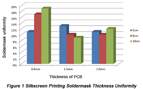
The result can be concluded as the follows:
a. For boards with the thickness of 0.8mm, the silkscreen ink thickness of nail bed with spacing of 5.0m between copper nails can reach 11%, which is better than that of 8.0cm and 10.0cm.
b. For boards with the thickness of 1.5mm and 2.0mm, the silkscreen ink thickness of nail bed with spacing of 5.0cm, 8.0cm and 10.0cm between copper nails is nearly the same.
c. Suitable reduction in terms of spacing between nail beds leads to obvious improvement of ink thickness uniformity of thin boards.
• Wet film thickness change trend of all test points
Based on the analysis on ink thickness change rules of each test point, the functionality of decreasing nail distribution spacing leads to the following result to improve the soldermask thickness uniformity:
a. Wet film thickness fluctuates with the changes of test positions. At the position with copper nail supporting at the bottom such as 1, 5, 9, 13, 21, 25, 29, wet film thickness is illustrated as the minimum value in the category. At the position far from copper nail supporter such as 3, 7, 11 (12), 15, 19 (20), wet film thickness is illustrated as the maximum value in the category.
b. At the place with copper nails supporting, wet film thickness is relatively low with board surface having no evident reduction while at the place far from copper nail supporters, wet film thickness is relatively high.
c. Relatively great deformation takes place to thin boards in the process of silkscreen printing while relatively small deformation takes place to thick boards. Therefore, thick boards with thickness of 1.5mm and 2.0mm are relatively flat on the surface.
• Relationship between wet film thickness and measurement position and supporting point
The relationship between wet film thickness and measurement position and supporting point can be summarized as follows:
a. For different spacing between nail distributions, the ink thickness of boards with different thickness increases with the improvement of the distance between test points and copper nails.
b. The thicker boards are, the smaller the change becomes with the improvement in terms of the distance between test points and copper nails. Therefore, the rigidity of board is relatively large and the distribution spacing can be relatively large.
• Dry ink thickness change on the surface of board
Dry ink thickness change on the surface of board can be concluded as the follows - the change trend of dry ink thickness and wet film thickness is basically the same, indicating that under the same test conditions, it's acceptable to replace dry ink thickness with wet film thickness. However, since the test result of wet film thickness is greatly influenced by the viscosity of ink, the thickness of wet film should be measured within 15 minutes after silkscreen printing.
Conclusion
With bare copper boards with the thickness of 0.8mm, 1.5mm and 2.0mm and nail beds with copper nail spacing of 5.0cm, 8.0cm and 10.0cm, thickness of wet film and dry ink is tested through cross matching with the following conclusion:
a. Ink thickness uniformity can be evidently improved when spacing between nail beds on thin boards (0.8mm thick or thinner).
b. Wet film thickness and dry ink thickness maintain stable, indicating the acceptability of on-line measurement using wet film thickness tester and ink film thickness monitoring.
Helpful Resources
• Design Requirement of SMT PCBs Part Two: Settings of Pad-Trace Connection, Thru-Holes, Test Point, Solder Mask and Silkscreen
• Effective Measures to Improve Solder Mask Plugged Via Manufacturing Technology
• Full Feature PCB Manufacturing Service from PCBCart - Multiple Value-added options
• Advanced PCB Assembly Service from PCBCart - Start from 1 piece


