



For most fine-pitch BGAs, NSMD (non-solder-mask-defined) pads are the better default. The copper sets the land size, the solder wraps the pad edge, and the joint usually lasts longer under thermal cycling. SMD pads still have a place on larger parts in products that get dropped or flexed, and on corner balls. Via-in-pad is worth paying for once a dog-bone via no longer fits between the balls, which usually happens somewhere around 0.5 mm pitch. When you use it, the via has to be filled and plated over, never left open.
What’s the real difference between SMD and NSMD pads?
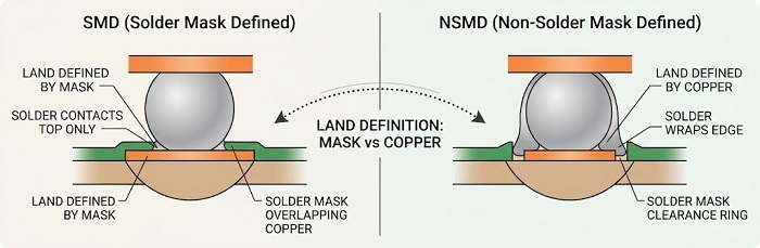
The difference is which layer defines the land. On an SMD pad it’s the solder mask opening. On an NSMD pad it’s the copper.
With SMD, the copper is drawn larger than the land you want, and the mask overlaps its edge. Solder only wets the exposed top surface. With NSMD, the copper is the land, and the mask opening is pulled back so a thin ring of bare laminate shows around it. Solder wets the top and the sidewalls of the copper.
That one geometric detail drives almost every other trade-off, including where the joint breaks when it does fail.
| SMD pad | NSMD pad | |
|---|---|---|
| What defines the land | Solder mask opening | Copper etch |
| Solder contact | Top surface only | Top surface plus copper sidewall |
| Land size controlled by | Mask registration and exposure | Copper etch tolerance |
| Pad adhesion | Mask overlap holds the pad edge down | Copper-to-laminate bond only |
| Where it tends to fail | In the solder near the mask edge, often at the intermetallic layer | Pad peeling or laminate cratering under the pad |
| Paste printing | Mask overlap seals against the stencil, so paste volume is more repeatable | Less stencil gasketing; more margin if the print is slightly off |
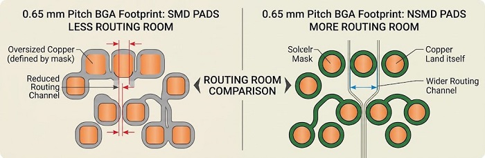
| Routing room between pads | Less (copper is oversized) | More (copper is the land itself) |
| Rework | Pads resist lifting; residual solder can sit against the mask edge | Easier to dress flat, but pads lift more easily if overheated |
Two of these rows deserve a closer look.
Tolerance first. On an SMD pad, mask misregistration shifts or shrinks the land itself. On an NSMD pad, it only changes the width of the clearance ring, as long as the mask never lands on the copper. That’s why NSMD lands are more consistent ball to ball at fine pitch. The flip side is that NSMD puts the burden on copper etching, so an undersized pad from etch variation goes straight into the joint.
Paste printing second. SMD has a real advantage here that often gets overlooked: the mask lip forms a small cavity that the stencil seals against, so paste release tends to be more repeatable. If you go NSMD at very fine pitch, aperture design and print setup matter more. The minimum mask clearance to hold around an NSMD pad depends on the board build, so confirm with our engineering team before you lock the library footprint.
Which one should you pick for your pitch?
Start from the package vendor’s land pattern, treat NSMD as the default, and switch to SMD only when you have a mechanical or printing reason.
Most BGA datasheets give the pad diameter and mask opening the vendor qualified the part with, sometimes in both SMD and NSMD versions. Use those numbers rather than a generic library footprint. If the datasheet is silent, a common starting point for NSMD is a copper land roughly 20% smaller than the nominal ball diameter, with IPC-7351 scaling that reduction to the ball size. For SMD, the copper is usually drawn close to the ball diameter and the mask opening provides the reduction.
From there, pitch narrows the choice:
At 1.0 mm and 0.8 mm, both types fit. NSMD is the default; SMD makes sense when the board will see shock or flex and pad lift is the failure you’re worried about.
At 0.65 mm and 0.5 mm, NSMD is usually the better fit because the extra routing room between lands is what makes escape possible.
At 0.4 mm and below, follow the datasheet closely. Some wafer-level and chip-scale packages specify NSMD and some specify SMD, because at that pitch the mask web between openings and paste repeatability can matter more than joint shape.
A hybrid footprint is also a legitimate choice. Board flex concentrates strain at the package corners, so using SMD for the corner balls (or the outer row) and NSMD everywhere else reinforces the weakest locations without giving up routing room in the middle.
One practical warning. We regularly receive Gerbers where the library had a negative mask expansion set by accident, which quietly turns an intended NSMD footprint into SMD. Overlay the mask and copper layers on every BGA before release, and if certain parts must stay SMD, say so in the fab notes by reference designator so nobody “corrects” the mask during CAM. On standard FR4, our fabrication capability covers BGA pitch down to 0.2 mm, but at the fine end, pad type, fanout and stackup are one decision, so send the package drawing with your first inquiry.
Does pad type decide whether a BGA survives drop and flex?
Not on its own. Pad type changes where a joint fails, but it rarely decides whether it fails when the board is flexing too much.
An SMD pad anchors the copper, so under overload the crack tends to run through the solder. An NSMD joint has more solder contact, so the solder holds better, and the weak point moves down to the pad-to-laminate bond. Swapping one for the other moves the failure location without removing the stress that caused it.
If a BGA keeps cracking in drop or vibration testing, look at the mechanics first: mounting screws or connectors close to the package, standoff spacing, board thickness, and whether the part needs underfill or corner bonding. A filled and capped via under an NSMD pad can help a little, since the plated barrel ties the pad into the board, but we treat that as a secondary benefit, not a fix for board flex.
Dog-bone fanout or via-in-pad?
Use dog-bone fanout wherever the geometry allows, and move to via-in-pad when a via and its pad no longer fit between four balls with a usable mask web left over.
A dog-bone places the via at the center of four lands and connects it with a short trace. The space available is set by the diagonal, which is the pitch multiplied by √2. Subtract one land diameter from that diagonal, and what’s left has to hold the via pad plus clearance on both sides.
| BGA pitch | Diagonal (pitch × √2) | Starting point for fanout |
|---|---|---|
| 1.0 mm | 1.41 mm | Dog-bone with through vias is comfortable |
| 0.8 mm | 1.13 mm | Dog-bone still works; check via pad size against land size |
| 0.65 mm | 0.92 mm | Dog-bone is tight; inner rows may not escape |
| 0.5 mm | 0.71 mm | Via-in-pad or laser microvias for inner rows, often an HDI stackup |
| 0.4 mm and below | 0.57 mm or less | Via-in-pad with laser microvias is the normal route |
Pitch isn’t the only trigger. A large array at 0.8 mm can run out of escape channels for the inner rows even when each individual dog-bone fits. Via-in-pad also shortens the path from a power ball to its plane, which helps when inductance is the real constraint.
The cost is extra steps: drilling, filling, planarizing and plating over the fill. Via-in-pad on a 1.0 mm BGA is rarely worth it unless you need that escape for a dense inner array or a lower-inductance power path. At 0.5 mm and below it’s often the cheaper option overall, because the alternative is more layers. On standard FR4 we support via-in-pad, resin plugging and blind/buried vias, with laser-drilled holes down to 4 mil, so you can put microvias in pad on the fine-pitch parts and keep through vias elsewhere.
Why must via-in-pad be filled and capped?
An open via in a BGA land pulls solder away from the joint and traps gas, so the via has to be filled and plated over to make the land flat and solderable again.
During reflow, molten solder wicks down the barrel. Paste volume was fixed at printing, so whatever disappears into the hole is missing from the joint. The result is a starved joint, a misshapen ball, or an intermittent open that shows up after some thermal cycles. Flux and air in the barrel are the second problem: they expand at reflow temperature and push into the molten ball, which is how you get large voids sitting right over the via. Tenting doesn’t help, because the via sits inside the land.
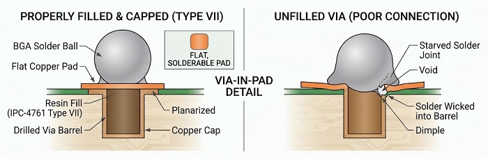
Plugging without capping only does half the job. Resin doesn’t wet, so the ball lands on a non-solderable spot in the middle of the pad, and any dimple left in the fill becomes a void pocket. The process that works is resin fill, planarize, then copper plate over the top, which IPC-4761 describes as a Type VII via. That’s how we build via-in-pad: the hole is plugged with resin before copper plating, so the finished land is flat and solderable.
Put two things in writing on the fab drawing. Call out the treatment explicitly, for example “via-in-pad, IPC-4761 Type VII, non-conductive resin fill, planarized and copper capped.” And if your design needs a limit on dimple or protrusion over the cap, state it and confirm with our engineering team that it fits the build. For laser microvias, copper-filled vias are an alternative; whether that suits your stackup is also something to confirm with our engineering team.
How do we verify BGA joints after reflow?
We verify BGA joints with X-ray, because no optical method can see under the package body.
The checks start earlier than that. 3D SPI measures paste volume and height on every BGA land, which is where many later defects begin, especially on NSMD lands at fine pitch. After placement and reflow on the JTR-1200D-N oven, 3D AOI confirms package position and checks the joints it can see at the periphery. Then the boards go to offline X-ray for the hidden array.
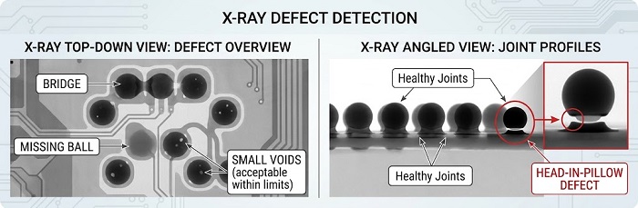
On the X-ray images we look for bridges, missing or misshapen balls, opens and voids. On via-in-pad designs we pay extra attention to voids sitting over the via location, because that pattern points to a fill or cap problem rather than a paste or profile problem. Head-in-pillow is the hard one. It can look acceptable on a top-down image, so angled views and electrical or functional test are what usually catch it.
Tell us your void acceptance criteria at the quote stage. Our default workmanship standard is IPC Class 2; if your drawing calls for different BGA void criteria, flag it early so inspection is set up against your numbers.
BGA pad checklist
| Item | What to check | Why it matters |
|---|---|---|
| Land pattern source | Pad and mask values taken from the package datasheet | Generic library footprints often don’t match the qualified land |
| Pad type | NSMD by default; SMD only with a stated reason | Joint fatigue life vs pad adhesion |
| Mask expansion | Overlay mask on copper for every BGA | Catches accidental SMD conversion |
| Fab notes | SMD parts listed by reference designator | Stops mask changes during CAM |
| Corner balls | Decide on SMD corners, underfill or corner bonding | Board flex strains the corners first |
| Mechanical stress | Screws, connectors and standoffs kept away from the package | Pad type alone won’t survive excessive flex |
| Fanout method | Diagonal minus land diameter leaves room for via pad plus clearance | Decides dog-bone vs via-in-pad |
| Via treatment | Via-in-pad called out as filled, planarized and copper capped | Open or uncapped vias cause starved joints and voids |
| Stencil apertures | Referenced to the actual land (mask opening for SMD, copper for NSMD) | Wrong reference changes paste volume |
| Inspection criteria | Void limits and workmanship class written on the drawing | Inspection follows your spec, not an assumption |
FAQ
If I change a footprint from SMD to NSMD, do I need a new stencil?
Usually yes. The solderable area and paste release both change, so we recheck aperture sizes whenever a revision changes pad type.
Which surface finish works best on fine-pitch BGA lands?
A flat one, such as ENIG or OSP. HASL leaves a domed surface that prints poorly as pitch drops.
What happens to NSMD pads during BGA rework?
They lift more easily, because no mask holds the pad edge. If you expect field rework, consider SMD corners.
What should a fab note for via-in-pad include?
Via size, fill material, “planarized and copper capped,” any dimple limit, and which parts or nets it applies to.
Is via-in-pad cheaper than adding layers?
For a single fine-pitch BGA it often is; for several large arrays, an HDI stackup may cost less. We can quote both from the same Gerbers.
<a class="download-bom-btn" href="https://www.pcbcart.com/assembly">Get a PCB Assembly Quote</a>
Helpful Resources


