Recent years has witnessed miniaturization, integrity and modularization of electronic products, leading to the escalation in terms of assembly density of electronic components and decrease in terms of effective thermal dissipation area. Therefore, thermal design of high-power electronic components and thermal dissipation problems at board level become so prevalent among electronic engineers. For FPGA (field programmable gate array) system, thermal dissipation is one of the pivotal technologies determining whether the chip is capable of normally working. The purpose of PCB thermal design is to decrease the temperature of components and the board through suitable measures and methods in order to make system work under suitable temperature. In spite of numerous measures to dissipate heat of PCBs, some requirements must be taken into account such as thermal dissipation cost and practicability. This article comes up with thermal design methods for PCBs controlled by FPGA system based on the analysis of the practical thermal dissipation problems to ensure the excellent thermal dissipation capability of FPGA system control board.
FPGA System Control Board and Thermal Dissipation Problem
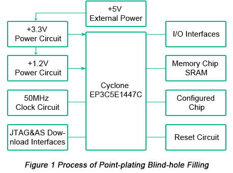
The FPGA system control board used in this article mainly consists of control chip FPGA (EP3C5E144C7 with QFP package of Cyclone III series by Altera®), +3.3V and +1.2V power circuits, 50MHz clock circuit, reset circuit, JTAG and AS download interface circuit, SRAM memory and I/O interface. The structure of FPGA system control board is displayed in Figure 1 below.

Heat sources of PCB controlled by FPGA system derive from:
• Numerous types of power supplies power for the control board such as +5V, +3.3V and +1.2V and power modules will generate large amount of heat when working for a long time. Power modules won't normally work unless suitable measures are effectively taken.
• The clock frequency of FPGA on the control board is 50MHz with high density of PCB routing. The escalation of system integrity leads to high system power consumption and necessary thermal dissipation measures should be made to FPGA chip.
• The PCB substrate generates heat by itself. Copper conductor is among the basic materials of PCBs and copper conductor circuit will generate heat with the exchange of current and power consumption.
Based on the analysis in terms of heat sources from circuit system controlled by FPGA control board, necessary measures to dissipate heat need to be taken to FPGA control board in order to increase the stability and reliability of the whole system.
Thermal Design of PCB Controlled by FPGA Chip
1. Thermal design of power
FPGA system control board is connected to +5V external direct current (DC) power that is required to supply a current of more than 1A. LDO chip LT1117 (with small SOT-23 SMD package) is picked up as the power module that is capable of transforming +5V DC power into +3.3V VCCIO interface voltage and +1.2V VCCINT VCORE.
According to the analysis above, two LT1117 chips are needed in the process of power circuit design so as to meet the voltage requirements of +3.3V and +1.2V by FPGA. Measures to dissipate heat of power modules in the process of PCB design include the following aspects:
• To ensure fast thermal dissipation of power module that supply power to FPGA chip, heat sink should be added to LDO chip when necessary.
• Since power module generates heat after long-time working, certain distance must be maintained between adjacent power modules. The distance between two LDO chips LT1117 should be kept 20mm or more.
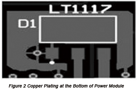
• To conduce to thermal dissipation, copper plating should be carried out independently on the place of LDO chip LT1117 as shown in Figure 2.

2. Thermal design of through holes
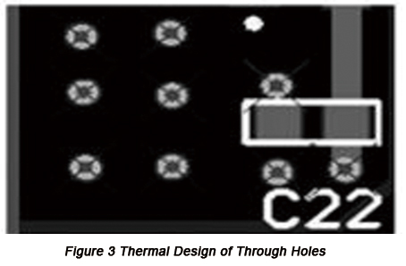
At the bottom of components with large amount of heat production on PCBs or near them should be placed some conductive metal vias. Thermal dissipation vias are small holes penetrating PCB with a diameter in the range from 0.4mm to 1mm and with the distance between vias in the range from 1mm to 1.2mm. Vias penetrating PCB make the energy at the front quickly passed to other thermal dissipation layers so that components on the hot side of PCB are instantly cooled down and thermal dissipation area is increased effectively and resistance is decreased. Finally, power density of PCB can be improved. The thermal design of through holes is displayed in Figure 3 below.

3. Thermal design of FPGA chip
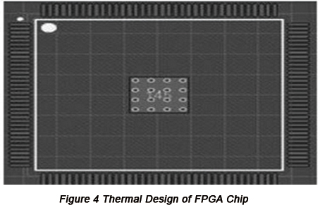
The heat of FPGA chip mainly comes from dynamic energy consumption such as VCORE and I/O voltage energy consumption, energy consumption produced by memory, internal logic and system and energy consumption produced by FPGA while controlling other modules (video, radio modules for example). When design FPGA chip QFP package, a copper foil is added to the center of FPGA chip with a size of 4.5mmx4.5mm and several thermal dissipation pads are designed. Heat sink can be added when necessary. The thermal design of FPGA chip is displayed in Figure 4 below.

4. Thermal design of plating copper
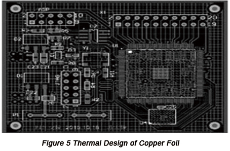
Plating copper on PCB can both increase the anti-interference capability of circuits and promote thermal dissipation of PCBs. PCB design based on Altium Designer Summer 09 usually features two types of plating copper: large area plating copper and grid shaped plating copper. Large area strip shaped plating copper features a defect that long-time working of PCB can lead to much heat generation, which will make strip-shaped copper foil expand and fall off. Therefore, in order to obtain excellent heat dissipation capability of PCB, copper plating should be implemented with grid shape and the connection between grid and ground network of circuit so that the shield effect of system and thermal dissipation performance will be improved. The thermal design of plating copper is displayed in Figure 5 below.

Thermal design of circuit boards is playing a pivotal role in determining working stability and reliability of PCBs and the determination in terms of thermal design methods is the most important consideration. This article discusses some measures to dissipate heat of PCB controlled by FPGA system and suitable method should be picked up with the consideration of cost and practicability.
Helpful Resources
• The Most Comprehensive Principles of Thermal Design for PCBs
• PCB Thermal Design Considerations
• Design of High-Power PCB in High Temperature Environment
• Metal Core PCB an Ideal Solution to Thermal Issues in PCB and PCBA
• Full Feature PCB Manufacturing Service from PCBCart - Multiple Value-added options
• Advanced PCB Assembly Service from PCBCart - Start from 1 piece


