Right now, high-speed PCB design has been widely applied in so many fields as telecommunication, computer and graph and image processing and all high-tech value added products are designed towards low power consumption, low electromagnetic radiation, high reliability, miniaturization and light weight. To obtain those targets, through-hole technology (THT) design and implementation is of extreme significance in high-speed PCB design.
Through-Hole Technology
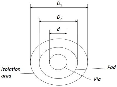
Through hole is one of essential parts for multi-layer PCB design. A through hole is composed by three parts: via, pad and isolation area of power plane, which can be demonstrated in the following image. THT is obtained by plating a layer of metal on hole wall in a way of chemical deposit so that copper foil from each internal layer or plane of a circuit board can be connected with each other. Two sides of through holes are generated in the shape of an ordinary pad, both of which can be directly connected with tracing on top and bottom layers and can be maintained unconnected as well. A through hole plays a role in electrical connection, fixation and positioning components.

As far as THT is concerned, through holes are generally classified into through-hole via, blind via and buried via:
a. Through-hole via goes through all layers of a circuit board, applicable for internal interconnection or playing a role as a positioning hole. Since through-hole vias are accessible in technology with a low cost, they are widely applied by most PCBs.
b. Blind via refers to the hole responsible for the connection between surface traces and internal traces below with certain depth. Ratio between via depth and via diameter usually doesn't exceed a certain value.
c. Buried via refers to connecting via located in internal layers, which cannot be seen from the appearance of a PCB board because it fails to be expanded to the surface of circuit board.
Both blind vias and buried vias are located in internal layers of circuit board and they are generated prior to lamination.
Parasitic Capacitance in THT
Through holes feature parasitic capacitance to the ground. Diameter of isolation via on ground plane is D2; diameter of through-hole pad is D1; thickness of PCB is T; dielectric constant of substrate material is ε. Then, parasitic capacitance of through holes can be calculated by formula C=1.41εTD1/(D2-D1)
The leading influence of parasitic capacitance on circuit is to prolong rise time of signals and lower circuit running speed. Thus, the lower parasitic capacitance is, the better.
Parasitic Inductance in THT
Through holes feature parasitic inductance as well. In the process of high-speed digital circuit design, hazards resulting from parasitic inductance are usually larger than those by parasitic capacitance. Parasitic series inductance will weaken the functions of bypass capacitance and reduce the filtering effect of the whole power system. When inductance of a through hole is indicated as L, through hole length as h, diameter of via as d, parasitic inductance of through hole can be figured out by conforming to formula L=5.08h[In(4h/d)+1]
Based on that formula, through hole diameter is seldom associated with inductance and the biggest element affecting inductance is through hole length.
Non THT (includes blind via and buried via)
When it comes to non THT, applications of blind via and buried via are capable of dramatically reducing PCB size and quality including layer count, improving electromagnetic compatibility (EMC) and getting cost minimized. Moreover, design task will become much easier. In traditional PCB design and PCB manufacturing process, through holes usually bring forward many issues. Firstly, they account for majority of effective space. Second, too high density of through holes brings a challenge towards internal tracing of a PCB board.
In PCB design, although the size of pad and through holes is constantly reduced, aspect ratio will rise when board thickness goes down non-proportionately and reliability will be reduced when aspect ratio increases. With the maturation of laser drilling technology and plasma dry etching technology, non-THT small blind vias and buried vias have become another possibility. When the diameter of those holes is 0.3mm, parasitic parameters will be one tenth of that of traditional vias with PCB reliability going up.
With non-THT applied, number of large through holes will go down on PCB board, so more space can be left for tracing. Rest space can be used as massive-area shielding in order to improve EMI/RFI performance. Moreover, more rest space can be also used as partial shielding for internal components and key network cables so that they can feature optimal electrical performance. The application of non-THT vias makes it easier for component pins to penetrate through so that tracing can be easier for high-density pin components such as BGA (ball grid array) components.
THT Design in Ordinary PCBs
Parasitic capacitance and parasitic inductance seldom feature influence on through holes during ordinary PCB design phase. As far as 1 to 4-layer PCB design is concerned, through holes with diameter such as 0.36mm, 0.61mm or 1.02mm can be selected respectively for via, pad and isolation area in ground plane. Some signal traces with special requirement can depend on through holes with diameters of 0.41mm, 0.81mm and 1.32mm.
THT Design in High-Speed PCBs
In accordance with parasitic properties of THT mentioned above, we can see that THT that looks simple tends to bring forward large negative effect to circuit design in high-speed PCB design. To reduce the bad effect deriving from parasitic effect of THT, the following tips are provided as a reference:
a. Suitable THT size should be picked up. When it comes to PCB design with multiple layers and ordinary density, THT should be picked up with through hole parameters being 0.25mm, 0.51mm and 0.91mm respectively for vias, pad and isolation area. High-density PCBs can also select through holes with parameters being 0.20mm, 0.46mm and 0.86mm for vias, pad and isolation area. Non-THT is also selective. For through holes concerning power or ground, large-size through holes can be selected to reduce impedance.
b. The bigger isolation area in power plane is, the better. As far as through hole density is concerned, the value of D1 is usually the sum of D2 and 0.41mm.
c. It's optimal to arrange signal traces not across layers, that is, number of through holes should be minimized.
d. Thinner PCB is leveraged to be beneficial to parasitic parameter reduction.
e. Through holes should be placed as closely to power and ground pins as possible and lead between THT and pins should be as short as possible because they will lead to inductance improvement. Furthermore, leads of power and ground can be as thick as possible to get impedance decreased.
Of course, specific issues should be specifically analyzed during PCB design phase. Two other aspects can never be avoided: cost and signal quality. Balanced considerations should be taken during high-speed PCB design to capture optimal signal quality with acceptable cost.
High-speed PCB design requires effective THT handling to minimize parasitic effects and enhance signal integrity. Designs that incorporate new concepts like blind and buried vias provide greater efficiency, smaller size, and reliability for modern electronics.
PCBCart provides expert PCB solutions with expertise in THT and state-of-the-art via technologies, ensuring precision and high-level performance. Our tailored approach caters to diverse requirements, offering low-cost, best-in-class designs. Trust PCBCart for your high-performance PCB requirements. Request a quote now and leverage our expertise to boost your electronic projects.
Request Your Advanced PCB Layout & Design Quote
You may also interested in:
• How to Design Blind/Buried Vias in High-Speed Digital Circuits
• Should Non-Functional Pads be Removed or Kept in Vias of High-Speed PCB?
• Research on High-Speed PCB Design in Embedded Application System
• How to Design Image Planes for High-Speed PCBs
• Full Feature PCB Manufacturing Service from PCBCart
• Advanced Turnkey PCB Assembly Service from PCBCart


