High-speed signals is a hot topic that can't be avoided by communication industries. With the increase amount of transmitted information and transmission speed rate, high-speed signals have gradually become significant. High-speed PCB is a loading board of high-speed signals and its material selection, manufacturing technology and routing design all affect quality of high-speed signals. Non-Functional Pad, aka NFP, is a technological method to manufacture high-speed PCB while insertion loss is one of the most important parameters indicating signal quality. To remove or to keep NFP has been an inevitable discussion topic between engineers and manufacturers. This article analyzes influence of NFP on insertion loss of high-speed signals from the perspective of manufacturing procedure in an experimental method, and guides you to the answer of whether to remove or to keep unused pads.
Introduction of NFP
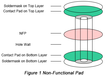
Non-functional pads are pads on internal or external layers that are not connected to any active conductive patterns on the layer. NFP has no influence on any electrical signal transmission but it is capable of strengthening copper adhesion on hole wall. NFP can be displayed in Figure 1 below.

Adding NFP means providing metal attachment points prior to PTH (Plated Through Hole) copper, so lots of manufacturers tend to add NFP in order to ensure better effect of PTH copper in the process of multi-layer PCB manufacturing .
Experiment Design
In this experiment, the same CCL (Copper Clad Laminate) material is selected. All PCBs contain 20 layers among which routing are implemented on the third and eighteenth layer. Insertion loss can be compared between adding NFP (Scheme 1) and removing NFP (Scheme 2) in order to ensure whether NFP has influence on signal quality. Because many uncertain elements do exist in the process of PCB manufacturing, the key parameters have to be inspected apart from insertion loss so as to guarantee no other influence elements are mixed into manufacturing.
Influencing Elements Inspection
• Impedance consistency inspection
In the signal loss test, signal reflection tends to be generated due to inconsistent impedance, which will finally influence test result of insertion loss. As a result, correctness of insertion loss test directly depends on the quality of impedance consistency. Characteristic impedance test is implemented respectively according to Scheme 1 and Scheme 2 and the obtained characteristic impedance value is summarized in below table.
|
Test Scheme
|
Test Layer
|
Characteristic Impedance (Ohm)
|
|
Scheme1
|
3rd layer
|
113.03
|
|
Scheme2
|
3rd layer
|
112.71
|
|
Scheme1
|
18th layer
|
111.93
|
|
Scheme2
|
18th layer
|
114.07
|
Based on above table, it can be seen that impedance difference falls within 5% between two schemes with a conclusion that influence of characteristic impedance on loss test can be neglected.
• Elements influencing insertion loss inspection
Insertion loss is composed by dielectric loss and conductor loss. Because the same material and light painting graphics are applied in two schemes inspected in this experiment, dielectric loss and conductor loss only result from PCB manufacturing. Next, both items will be respectively analyzed in order to ensure non-influence on PCB manufacturing.
a. Dielectric loss inspection
Application of adhesive bonding sheet in multi-layer stacking will produce some resin recession and different amount of resin recession leads to differences between dielectric loss. In terms of uncertainty of resin recession on adhesive bonding sheet, x-section analysis has to be implemented after stacking up in order to totally eliminate influence owing to difference in terms of resin recession amount.
Through the analysis, it can be summarized that core thickness of upper layer and lower layer of the two schemes is respectively 139.8μm and 135.2μm. After stacking up, thickness of adhesive bonding sheet is respectively 257.4μm and 251.9μm. The maximum thickness difference falls within 6μm, catering to manufacturing tolerance requirement and insertion loss won't be influenced due to the dielectric loss.
b. Conductor loss inspection
Conductor loss, then, is related with length and width of lines, surface roughness and lateral erosion during PCB manufacturing process in test circuit. In the two schemes of this experiment, circuit design is the same with the influence of line length eliminated. Brown effect, concentration of etching solution and water pressure all have influence to surface roughness. To avoid these complicated elements, circuit consistency is directly judged from the final result.
Through the experiment, transmission line width is measured to be respectively 168μm and 166μm with the application of Scheme 1 and Scheme 2 and transmission line height 18.3μm and 18.9μm. Surface roughness both stay at 2.5μm. All the data indicate that conductor loss is basically similar in terms of transmission line manufacturing so that influence of conductor loss on insertion loss can be eliminated.
NFP Influence Analysis
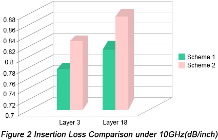
Starting from generation source of dielectric loss and conductor loss, coupled with generation principle of insertion loss, a series of inspections are implemented in terms of PCB manufacturing consistency in order to ensure only one variable, which is NFP, occurs in the two schemes. According to FD (Frequency Domain) method in IPC-TM650-2.5.5.12, Scheme 1 and Scheme 2 are tested with the result displayed in Figure 2 below.

As a result of the only variable, NFP, influence of NFP on signal insertion loss can be approximately judged. Scheme 1 removes NFP while Scheme 2 keeps NFP. It can be seen from the figure above that either layer 03 or layer 18, insertion loss test result in Scheme 1 is all smaller than that of Scheme 2, which indicates that adding NFP will strengthen signal insertion loss.
Based on this experiment, insertion loss difference maintains at approximately 9% between two schemes. Figure 3 is a primary grading on a famous communication terminal material.

Based on Figure 3, it can be seen that very little insertion loss difference does occur between all ranks of materials. If the insertion loss inspected in this experiment just falls within the category of threshold, material grade will be decreased by NFP, which will greatly influence the whole production line from material manufacturer to end.
Conclusion
When comes to high-speed PCBs, multi-layer PCBs are inevitable the development trend and through via manufacturing is the first problem. NFP features great improvement to PTH copper in the process of manufacturing PCB via wall and plays an effective role in stopping via copper from falling and dealing with quality problems such as via wall crack. Eliminating other influencing elements, the variable of NFP is considered in this article and influence of NFP on insertion loss is analyzed so that it is capable of providing some reference to material manufacturer, PCB manufacturer and terminal manufacturer in terms of high-speed PCB design.
PCBCart is a leader in providing high-precision PCB manufacturing solutions that are tailored to satisfy the strict needs of high-speed applications. Our experience ensures superior design, part selection, and manufacturing processes that minimize insertion loss and optimize signal performance. With our advanced technology and rigorous quality assurance, we help you achieve greater product performance. Order a quote now from PCBCart and benefit from working with a leader in advanced PCB solutions.
Get Your Custom High-Precision PCB Quote Now
Helpful Resources
• Via in pad (VIP) Technology Introduction
• High-Speed Layout Tips
• High-Speed PCB Routing Techniques to Reduce the Influence of EMI
• Research on High-Speed PCB Design in Embedded Application System
• Full Feature PCB Manufacturing Service from PCBCart - Multiple Value-added options
• Advanced PCB Assembly Service from PCBCart - Start from 1 piece


