Future PCBs (printed circuit boards) won't develop without innovation. To estimate and expect the future of PCB fabrication technology, it's optimal to implement a research on some great changes occurring to electronics products concerning PCB industry in recent years.
SiP and SLP
September of 2014 witnessed Apple's release of Watch S1 whose mother board takes advantage of SiP (system in package) that is different from any layer or high-level HDI (high density interconnect). Similar with S1, Watch S2 and S3 depend on SiP as well. When it comes to design parameters of specific PCB, layer count is 8; board thickness is 0.35mm; minimum trace/spacing is 0.02mm/0.02mm; the minimum pad size is 0.1mm.
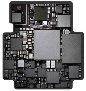
Image cited from iDB.
In 2017, Apple released iPhone 8, iPhone 8 plus and iPhone X whose main processors, A11, relies on FOWLP (fan-out wafer-level packaging) technology, whose motherboard takes advantage of SLP (substrate like PCB) and whose trace first depends on MSAP (modified semi-additive process) technology.
Therefore, based on PCB design for Watch S1, iPhone 8, iPhone 8 plus and iPhone X, it can be concluded that high-level HDI is developing towards load board trend. HDI develop trend towards load board can be also indicated by Samsung electro-mechanics on its introduction on HDI ultra-fine line technology that is demonstrated as below.
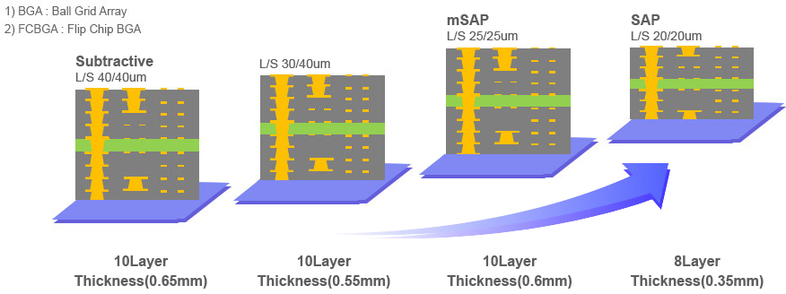
Image cited from SAMSUNG ELECTRO-MECHANICS.
FOWLP and FOPLP
September of 2016 witnessed Apple's release of iPhone 7 whose main processor A10 takes advantage of FOWLP technology that is also called InFOWLP technology. FOWLP is used to replace PoP (package on package), which means that substrate and package are no longer used.
FOPLP, short for fan-out panel level packaging, refers to chip placement on substrate to implement RDL (redistribution layer) packaging. A traditional way depends on bump and chip package on strip-based substrate. Generally speaking, a panel is composed by 8 to 10 strips. This is actually component embedment technology focused on in previous part of this article. But in this process only active components are participated.
FOPLP and FOWLP are two different directions on how active components are packaged, being a challenge to traditional packaging method. FOPLP belongs to board-level package and is carried out on the whole loading board while FOWLP belongs to wafer-level package and is carried out on wafer.
In accordance with the contrast analysis between SiP and SLP, FOWLP and FOPLP, it can be concluded that all the new technologies are both challenge and opportunity as far as HDI is concerned. As far as substrate is concerned, however, all the new technologies are challenges for it.
Printed Electronics
Printed electronics refers to electronics circuits combined by electronic components and circuits based on all kinds of printed technologies. Because printed electronics technology features advantages including low cost, numerous deformation, easy production, easy integration and environmental protection, it has been receiving attention from a large scale. Due to limit in terms of technology, however, it hasn't been produced in volume.
Technologies contributing to printed electronics manufacturing include: stencil printing, flexible bump printing, flat printing, grooving printing, jet ink printing, mold printing, imaging printing and laser imaging etc. Concerning materials include substrate material (majority is organic thin film), function materials (that is, oil including conductor material, semiconductor material, insulating dielectric material).
Because merits of printed electronics technologies are never avoided, it will bring forward more challenges to traditional PCB industry in the future.
Based on the analysis implemented above, possible technology development trend of PCB will be:
• HDI board loading (or SiP);
• Substrate packaging (or moduling);
• Printed electronics will constantly become prevalent.
Reach PCBCart for Custom PCB Production
Whatever circuit boards you need, simply reach PCBCart for production solution. We have been manufacturing PCBs since 2005. Our rich experience and highly-talented agents helps guarantee your circuit design being printed exactly as the way you designed, and within budget. You may reach our friendly agents on this page to discuss your project or get an online PCB quote by clicking below button.
Get Instant PCB Fabrication Quote
Helpful Resources
• Printed Circuit Boards Introduction and Categories
• A Brief Look At Industries Where PCBs Are Commonly Used
• What's Next for PCBs?
• PCBCart Full Feature PCB Fabrication Service
• PCBCart Offers Custom PCB Assembly Service as Well


