In the sustainable development of IC (integrated circuit) design and manufacturing, the prominence of some problems such as signal transmission delay and noise plays a role in influencing integrity of signals. Therefore, sufficient attention must be paid to the problems in the process of PCB design and process flow of electronic products must be supervised such as trial-producing and manufacturing steps. Besides, PCB design should undergo some improvement in order to solve these prominent problems under the traditional design module and to realize the reasonable application of EMC (Electro Magnetic Compatibility) technology. This article mainly discusses the application strategies of EMC technology in PCB design for electronic devices.
EMC Overview and Problems
EMC refers to a type of capability that devices or systems are capable of operating normally without being disturbed by electromagnetic interference and of refusing to provide electromagnetic disturbance to any part in the circuit environment.
When designing PCB of electronic devices, the problem of signal interference usually comes up with signal disturbance sources diversity. Therefore, during signal transmission, EMC technology with functions of isolation, filtration, shield and ground will help to improve the whole PCB design level.
In the process of applying EMC technology, in order to increase overall application effect, the quality of components must be tested. Specifically, in the process of EMC system construction, the components concerned by EMC technology must be tested in terms of voltage withstanding capability and capacity through experimental approaches. Meanwhile, in the process of experimental inspection, attention should be paid to the integrity of prominent problems and suitable dealing in the process of component application.
In PCB design, the main EMC problems include conduction interference, crosstalk interference and radiation interference.
• Conduction interference
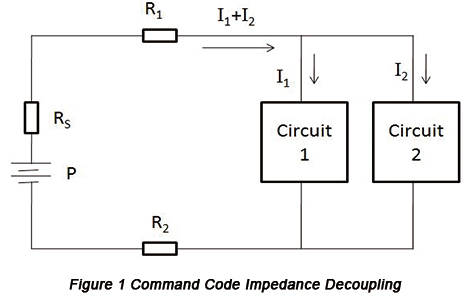
Conduction interference influences other circuits by lead decoupling and common mode impedance decoupling. For example, noise enters a system through power circuit whose supporting circuits will be influenced by the noise.

Figure 1 shows the noise decoupling through common mode impedance. Both Circuit 1 and Circuit 2 get the power voltage and ground loop through the same lead. If the voltage of either of the circuits suddenly needs improving, the other circuit will decrease because of the common power and the impedance between two loops.
• Crosstalk interference
Crosstalk interference refers to the interference from one signal line to an adjacent signal line, which usually takes place on the adjacent circuit and conductor and features mutual capacitance and mutual impedance between circuit and conductor. For example, a strip line on a PCB has a low level signal and when parallel wires are longer than 10cm, crosstalk will come up. Because crosstalk can be aroused by electricity field through mutual capacitance, by magnetic field through mutual impedance, the first and foremost problem is to determine which decoupling has the main role, electricity field (mutual capacitance) decoupling or magnetic field (mutual impedance). The product of power impedance and receiver impedance can be regarded as a reference, which depends on the configuration between circuits and frequency.
|
Product
|
Main Decoupling
|
|
<3002 |
Magnetic field |
|
>10002 |
Electricity field |
|
>3002, <10002 |
Magnetic or Electricity field |
• Radiation interference
Radiation interference refers to the interference led by the radiation released by free electromagnetic wave. The radiation interference in PCB refers to the common mode radiation interference between cables and inner lines. When electromagnetic wave shines on transmission lines, decoupling problem will come up from the electricity field to lines with the distributed small voltage sources classified into CM (common mode) and DM (differential mode). CM current refers to the current from two leads that have almost equivalent amplitude and equivalent phase position while DM current refers to the current from two leads that have equivalent amplitude but contrary phase positions.
EMC Application Strategies in PCB Design of Electronic Devices
• ESD (Electro-static discharge) Protection
When designing PCB of electronic devices, ESD has impact to the stability of current running by means of direct conduction or inductance decoupling, which leads to the necessity of ESD protection to meet the requirement of electronic production development. PCB designers of electronic devices must ensure EMC technology is ingrained in the process of PCB design of electronic devices. That is to say, in the process of developing new electronic products, plated-through holes should be positioned at PCB and in the process of plated-through holes design, outer circuit on metal shell should be connected with inner circuit and fixed screws have to be assembled at the connection. The ultimate goal is to establish excellent inner-outer equipotential environment in order to avoid the prominence of ESD that will lead to circuit failure. For example, some type of electronic devices emphasize the application of EMC technology and 6 plated through holes should be arranged in order to ensure the excellent connection between inner circuit and LCD enclosure so that overall PCB design has been substantially improved. Besides, this type of electronic devices arrange ESD protection components at the place of signal input and output and electrostatic ring has been assembled to it so as to avoid the prominence of ESD that possibly decreases the stability of circuit running.
• Decoupling Capacitor Configuration
In the process of PCB design of electronic devices, power system plays an important role in influencing signal integrity so the application of EMC theory must be emphasized. In the process of decoupling capacitor configuration, circuit running can be simulated during which the noise interference phenomenon can be mastered so that noise problem can be effectively controlled. Meanwhile, in the process of decoupling capacitor configuration, technicians are required to strictly inspect power filter capacitance input terminal that should be maintained in the range of 10 to 100F in order to meet the conditions of EMC technology. Besides, system frequency should be controlled less than 15MHz in order to increase the application level of electronic devices and decoupling capacitor configuration should be positioned at the place of integrated chip.
• Thermal Design
Thermal design is one of the most important elements that influence electronic devices' performance. Under the influence of heat radiation and ventilation, distance between components and heat source must be controlled within the standard range and heat degree of components must be inspected from time to time in the process of components assembly such as capacitors. Moreover, when assembling components with high power, make sure to place those componetns on top of PCBs so that the best thermal design can be carried out to increase the overall PCB design level.
• Line Length and Width Design
In the process of EMC design of electronic device PCBs, line width and length have direct relations with signal transmission efficiency. PCB designers should especially scrutinize the transmission delay effect based on which the best circuit design can be reached. Printed lead inductance effect leads to interference and the length of printed lead is proportional to interference effect so printed lead should be controlled in the short and wide condition to meet the developing requirement of new electronic devices. For example, in the process of the development of some type of electronic devices, design of line length and width is taken into full considerations so that the 9th pin XIN of EM78860 is placed at the position of oscillator and the lead at the place of DL16521 is kept short, all of which increases the overall EMC design level. Therefore, it's extremely necessary to emphasize the scientization and rationalization of line length and width to fully meet the development requirement of new electronic devices.
Based on the fast development of electronic devices, PCB design has been arousing more attention to the high efficiency and stability of PCBs, which leads to the emphasis on the role of EMC technology. The prominent problems concerning EMC technology should be dealt with from the perspectives of design of line length and width, decoupling capacitor configuration and ESD in order to reach the best design effect, based on which the substantial development of electronic devices design will be pushed.


