In the process of PCB design, PCB material selection mainly depends on the following elements: cost, electrical performance, machinability, heat withstanding capacity, UL certificate etc.
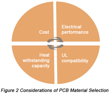
Material price influences the whole cost of PCBs; electrical performance of material is directly related with signal integrity; machinability and heat withstanding capacity of material determines reliability of PCBs; UL compatibility of material is the privilege of UL certificate application. Among all these elements to be considered, machinability, heat withstanding capacity and UL certificate should be considered in the process of PCB design of products in all fields.
For PCBs in communication network, however, PCB materials at different levels are required owing to requirements at different levels from high speed to low speed. Electrical performance and material cost usually interact with each other so that materials with higher class usually feature excellent electrical performance but with high cost as well. In addition, price difference occurs among materials with the same class due to different types of materials.
How to decide a type of material that is capable of both meeting the requirement in terms of electrical performance of PCB and taking cost control in consideration lies in accurate judgment and identification of Dk/Df that manifests electrical performance parameters, matching of copper foil with low roughness to ensure electrical performance and cost differences between all types of materials.
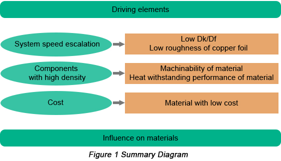
Therefore, in this article, two aspects, electrical performance and cost are analyzed in terms of PCB material selection.
• Identification and comparison between PCB materials in terms of electrical performance (Dk/Df)
In order to make selected material meet the requirement of signal integrity, the first task lies in judgment and comparison between PCB materials in terms of electrical performance (Dk/Df).
a. Comparison approaches and judgment standard of electrical performance between materials
Electrical performance comparison between materials from different suppliers should be implemented with the same test method and under the same condition to provide fairly objective reference.
Even though Dk/Df values of corresponding prepreg and core board are provided in specifications offered by suppliers, it's not acceptable or scientific to directly refer to the spec data. True electrical performance comparison between PCB materials should depend on experimental data since test method and test condition is different from one supplier to another. Even if the same test method is applied, difference will possibly still take place due to different operations.
The judgment standard of electrical performance of PCB materials is the values of Dk and Df and their stability at each frequency. Low Dk/Df will decrease insertion loss and it should be noticed that in increasingly high-speed design, Df is more important than Dk as a parameter. Stability refers to the fact that Dk/Df shouldn't be changed obviously with the increasing of test frequency, which is not beneficial to signal integrity. The following formula indicates the relationship between Dk/Df and insertion loss:

b. Comparison samples between materials based on practical test results
1). Sample test data accumulation
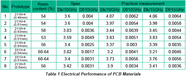
Materials in Class 0 and Class 1 display better electrical performance and they are only applied in super high-speed PCBs. Table 1 shows the result comparison between 8 materials in two classes after Dk/Df test.
2). Comparison on Dk
Based on Table 1, if comparison is carried out according to the data of spec, the sequence of Dk should be 6>3>5>7>8>4>2=1 in accordance with its influence.
However, under the same condition, the sequence of Dk should be 6>5>8>3>7>4>2>1 in accordance with its influence, which is a reasonable result. In addition, it can be concluded that with the rising of test frequency, Dk usually changes with it. Based on the test result, Dk of each material manifests excellent stability at 10GHz and 15GHz with its change within 0.03.
3). Comparison on Df
Based on Table 1, if comparison is carried out according to the data of spec, the sequence of Df should be 6>5>7>8>3>2=1>4 in accordance with its influence.
However, under the same condition, the sequence of Df should be 5>8>3>6>4>7>2>1 in accordance with its influence, which is a reasonable result. In addition, it can be concluded that with the rising of test frequency, Df usually rises as well. Based on the test result, Df of each material manifests excellent stability at 10GHz and 15GHz with its change within 0.0005.
4). Electrical performance comparison and judgment of materials
According to Part a in this section, material No. 5 features the best electrical performance since it has the best Df and relatively excellent Dk. Next is No. 8 since it is right after No. 5 in terms of Dk and Df. Then comes No. 3. Although No. 6 features the best Dk, Df is only ranged the fourth. Next come No. 4 and 7. Electrical performance is the worst for No. 1 material. In conclusion, the sequence of electrical performance should be 5>8>3>6>4>7>2>1.
• Application of copper foil with low roughness
The formula below indicates the relationship between roughness of copper foil and skin effect and conductor loss.
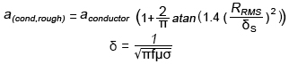
In this formula, acond,rough refers to the insertion loss of conductors; RRMS refers to roughness of copper foil; δ refers to skin effect; f refers to frequency; μ and σ refer to conductivity and permeability of material.
Based on this formula, it can be concluded that the increase of roughness of copper foil will lead to the increase of conductor loss. The roughness of ordinary copper foil is usually more than 6μm. Thanks to transmission requirement of high-speed signals, reverse-treated foil (RTF) and VLP copper foil are developed and applied with their roughness of copper foil approximately 3μm. Higher requirement on high-speed signals promotes roughness of 1μm to 2μm featured by HVLP or similar copper foil.
In the process of PCB material selection, copper foil with low roughness is configured to reduce insertion loss and improve electrical performance of material. Based on the experiment, it can be summarized that starting from No. 4 material, RTF or VLP copper foil should be picked up and it can be upgraded to HVLP or similar copper foil so that electrical performance of material can be increased, conductor insertion loss decreased. Difference of insertion loss resulting from difference of roughness of copper foil is becoming increasingly obvious with the escalation of frequency. Configuration of copper foil with low roughness is capable of reducing insertion loss in high-frequency situation.
• PCB material compatibility with signal integrity simulation and test verification and determination
a. Signal integrity simulation to verify compatibility of electrical performance of PCB material
Signal integrity simulation is capable of predicting system performance and evaluating compatibility of electrical performance of materials. Simulation comes in two forms: pre-simulation and post-simulation.
Pre-simulation, also called schematic simulation refers to simulation before design. The aim of pre-simulation lies in the awareness of characteristic impedance of transmission lines, through-hole capacitance effect and influence of spacing between lines on transmission signals, which will be good for PCB routing design. At this stage, Dk/Df of PCB material is also concerned, just initial assessment.
Post-simulation refers to correctness checking after stackup and routing design before PCB fabrication. It is implemented based on final design parameters, covering transmission quality simulation and crosstalk simulation. With flowchart of post-simulation added in PCB design process, based on result of post-simulation, it can be determined whether previous PCB material electrical performance is suitable or not.
b. Material compatibility determined by signal integrity test
Signal integrity test is carried out on the whole system is the checking on the performance of product. Material with low loss or low Dk/Df is an important element to be considered in the process of communication network PCB design. In high-speed design, Dk/Df of PCB material contributes a lot to dielectric loss since Df of PCB material is positively correlated with dielectric loss and Dk also contributes at some extent so that loss of the whole system is influenced. Design optimization based on Dk of material will influence impedance continuity that will directly affect return loss and crosstalk.
Since electrical performance of PCB material greatly influences high-speed equipment system, implementation of system signal integrity test including network signal quality, track collapse and electromagnetic interference is capable of helping to check compatibility of previous PCB material. The test methods cover impedance analysis meter, vector network analyzer and time domain reflector.
• PCB cost change resulting from differences between PCB materials
In order to select material with low cost from multiple types of materials, PCB cost change resulting from differences between PCB materials has to be fully aware.
Since each type of material has its own core board and prepreg, if price comparison is only implemented on one type of core board and prepreg or on limited types, deviation will be generated in the process of cost comparison between materials, which will mislead PCB material selection. Therefore, price comparison has to be implemented on all ordinary core boards and prepreg with average value figured out so that PCB price difference can be clear.
It's worth noting that PCB price is also influenced by other design parameters. This article only focuses on PCB cost decrease proportion brought by PCB material difference.
a. PCB cost difference caused by PCB materials with different electrical performance levels
Through the simulation, it can be concluded that application of material with low level causes more remarkable cost saving then that of material with high level.
b. PCB cost differences caused by optimal material selection in the same class
Even within the same class, price difference takes place among these materials. Under the privilege of electrical performance compatibility, material with price advantages should be first applied so that cost can be saved. For PCBCart, you can make use of PCB calculator in which different types of material can be picked up according to your design requirement. Of course, different selections of material lead to different quote results.
• Signal integrity simulation avoiding PCB material selection over design
In the process of PCB design, if material with high class is applied in products whose signal integrity can be fully reached by material with low class, PCB cost waste will be produced, which is called PCB material selection over-design.
Through type number integrity simulation, issue of over-designing can be avoided so that PCB material with suitable class can be picked up, promoting cost saving through lowering material class.
• Application of special design to improve insertion loss and signal transmission quality to increase possibility of using material with low class
a. Backdrill and blind via design
Backdrill and blind via design is capable of decreasing and eliminating signal transmission influence caused by through-hole plating because plating through holes can be regarded as a circuit that can improve signal transmission quality.
b. Surface finish
Based on some research about PCB surface finish, it can be verified that for high-speed PCBs, application of surface finish without nickel is helpful in decrease of insertion loss so that possibility of material with low class application can be increased. Both OSP and immersion silver can be applied by high-speed PCBs as surface finish. Moreover, OSP PCB features more benefits owing to its low cost.
c. Application of hybrid stack by materials with high class and low class to decrease material class
Since some key signal traces are just distributed on some layers in high-speed PCBs, material with low class or even ordinary material can be applied on core board without high-speed signal lines, which is capable of greatly decreasing cost.
In communications network devices, keeping high electrical performance with cost-effectiveness in material selection for PCB is crucial. Designers need to study parameters like Dk/Df and copper foil surface roughness in a way that they achieve the highest performance within budget constraints. With smart material selection, it becomes possible to enhance the functionality and cost-effectiveness of high-speed devices.
PCBCart specializes in offering customized PCB material solutions with the perfect blend of performance and cost-effectiveness. Our expertise and resources make it easy to select the most appropriate materials for your particular needs. Contact PCBCart today for detailed quotes and learn how we can support your PCB projects with our proficiency in design and manufacturing solutions.
Request Your Custom PCB Material Quote from PCBCart Now
Helpful Resources
• Printed Circuit Board Design Guide
• High Quality Standard PCB with 20+ Years of Experience
• Introduction to PCB and Different Types of Circuit Boards
• Design Requirement of SMT PCBs Part Four: Mark
• PCB Manufacturing Process – A Step by Step Guide
• FAQs | Professional PCB Manufacturer PCBCART