



Why Test Escape Rate Traces Back to Test Coverage, Not Chance
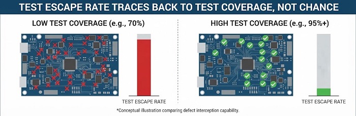
A test escape is a defect that passes through in-circuit test (ICT), functional test (FCT), or boundary-scan without being flagged, and shows up later — at final inspection, in the field, or worst case, inside a customer's system. Engineers often treat test escapes as a process-control problem: tighten the reflow profile, recalibrate the pick-and-place, add another AOI pass. Those fixes matter, but they don't move the number that actually determines whether a defect gets caught: test coverage.
Test coverage is the percentage of a board's nets, nodes, and functional blocks that a given test method can actually exercise. If a net has no probe access, no boundary-scan cell, and no functional stimulus path, no amount of tester sophistication will catch a short or open on that net. The defect isn't undetected because the tester is weak — it's undetected because the board was never designed to expose it.
Industry sources illustrate why this ceiling matters, even though they measure it two different ways. In-circuit test alone can intercept roughly 70–90% of manufacturing defects when test point access is adequate, with functional test covering the system-level behavior ICT cannot reach — that figure describes the defect types a single method reaches. Separately, commonly cited test-coverage benchmarks put overall test-strategy goals at 95%+ for high-reliability products versus 85–90% for consumer electronics — that figure describes the structural (net/node) coverage a full test plan aims for, combining multiple methods. The two numbers aren't directly comparable, but they point to the same conclusion: no single test method gets a design to the coverage level its product class requires, and the shortfall has to be designed for, not tested around.
This is why DFT belongs in layout review, not in the test department's post-mortem. By the time a board reaches the test floor, its testability is already fixed.
Testability Rules for Critical Nets
Test Point Exposure
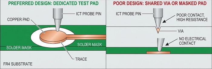
• Every net carrying power, reset, clock, or a single point of failure for a functional block should terminate in a dedicated test pad — not just a via, and not a component pad shared with several other measurement points.
• Minimum test pad diameter should match the probe technology in use (bed-of-nails vs. flying probe); flying probe tolerates smaller, tighter-pitch targets but adds cycle time, so the trade-off should be made deliberately, not by default.
• Test pads must sit on a single, probeable side of the board (typically the bottom for bed-of-nails fixtures) and stay clear of tall components, connectors, and mechanical hardware that would obstruct probe travel.
• Solder mask should not encroach on the test pad surface — a masked-over pad reads as an open to the tester even when the joint underneath is sound.
Isolated Net Design
• Where two components share a net for functional reasons (bus lines, ganged power rails), insert a series test point or a normally-populated 0-ohm link so a fault can be isolated to one side of the junction rather than reported as an ambiguous fail across both.
• If two power or ground domains are deliberately tied together by design, document that explicitly in the test procedure — otherwise an ICT program written to expect isolated domains will flag the intentional connection as a short, and a legitimate design gets treated as a defect.
• For analog nets with tight-tolerance components, keep the test point close to the component under test to avoid trace resistance and stray capacitance skewing parametric measurements.
Boundary Scan (JTAG) Reservation
• Reserve TCK, TMS, TDI, TDO, and TRST on a dedicated header or test-point cluster early in layout — retrofitting a boundary-scan chain after routing is largely impractical.
• Confirm every IEEE 1149.1-compliant device in the design is actually included in the intended scan path; one device left out of the chain breaks continuity testing for every device downstream of it.
• Boundary scan is not a substitute for full test coverage: it cannot properly test passive devices such as resistors and capacitors, cannot measure analog values or verify power integrity, and only covers interconnections between components that comply with the IEEE 1149.1 standard. Plan a complementary test method — ICT, flying probe, or functional test — for every passive network and analog stage the scan chain can't reach.
The Density Trade-off: Test Coverage vs. Component Count
High-density boards create a structural conflict: every square millimeter given to a test pad is a square millimeter not available for routing, decoupling, or component placement. On boards built for ATE interface cards, industrial control modules, or compact sensor front-ends, this trade-off is unavoidable — and DFT decisions need to be made component-by-component rather than by blanket policy.
• Prioritize test access by failure consequence, not by convenience. Nets that cause a total functional failure (power rails, reset, clock) earn dedicated test pads even if it costs routing channels; nets with a redundant or self-checking function downstream can tolerate reduced coverage.
• Expect full test point access to become impractical at high pin density and high-speed signaling. Implementing 100% test point access is difficult even when product margins could absorb the cost, particularly for high-speed differential signaling boards where test points are often not permitted, because a probe pad's stub length and capacitance would degrade signal integrity.
• Fall back to boundary scan or edge connectors for pin-starved areas, accepting the coverage limitations noted above rather than compromising a differential pair's routing to force a physical test point onto it.
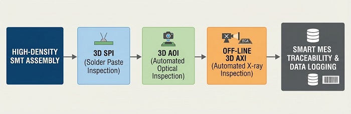
• Close the gap with inspection-based coverage where electrical test can't reach. For bottom-terminated packages such as BGAs and QFNs, closed-loop 3D SPI and 3D AOI catch paste and placement defects before reflow, and off-line X-ray inspection with oblique-angle capability verifies solder joint integrity and voiding after reflow — covering failure modes no test point budget would expose electrically.
• Use MES-level traceability to offset reduced point coverage. A Smart MES with UID-based traceability and laser marking won't catch a defect at test, but it lets an engineering team trace a field failure back to the specific board, panel, and process step — narrowing root-cause analysis when a low-coverage net turns out to be the failure mode months after shipment.
None of this replaces test coverage; it reallocates where coverage comes from — electrical test, optical/X-ray inspection, or traceability — based on what the board's density actually allows.
Where This Fits in This Series
This article sets out general-purpose DFT rules that apply across board types. A related article in this series looks specifically at how these principles play out in life-sciences PCBA designs, where component density, signal isolation, and test access carry additional constraints tied to the end application. Readers working on a diagnostic, monitoring, or lab-instrumentation board should treat this article as the DFT foundation and the life-sciences piece as the applied layer on top of it.
DFT Design Checklist
Before releasing Gerbers for assembly, confirm:
☐ Every power, reset, and clock net has a dedicated, unobstructed test pad
☐ Test pads sit on one probeable side and are clear of tall components and mechanical hardware
☐ Solder mask does not cover any test pad
☐ Shared or ganged nets have a test point or 0-ohm link enabling fault isolation
☐ TCK/TMS/TDI/TDO/TRST are broken out and every IEEE 1149.1 device is confirmed in the scan chain
☐ A complementary test method is assigned to every net or component the scan chain and ICT cannot reach
☐ High-density or high-speed areas have a documented fallback (boundary scan, inspection, or functional test) instead of a forced test pad
☐ Bottom-terminated packages (BGA/QFN) are covered by SPI/AOI/X-ray rather than left to electrical test alone
Get a File Review Before Tooling
If a board is heading toward layout release, submitting the Gerber and BOM — with the test point layer included, if available — through PCBCart's Free DFM Check alongside a PCB Assembly quote puts the file in front of an engineering reviewer before tooling starts. The Free DFM Check itself is built around manufacturability items — drill, signal/mixed-layer, power/ground, solder mask, and silkscreen checks — rather than test access specifically, so it's worth calling out the checklist items above in the quote notes if a DFT-focused look is wanted alongside the manufacturability pass. PCBCart is IATF 16949-certified for its HMLV PCBA assembly process, with 3D SPI/AOI, off-line X-ray, and Smart MES traceability lines that cover the BGA/QFN inspection and genealogy gaps this checklist calls out.
Helpful Resources
First Article Inspection Service on all PCB Assembly Orders
Comparison of AOI, ICT and AXI and When to Use Them during PCB SMT Assembly


