PCB successfully added to your shopping cart
Comparison of AOI, ICT and AXI and When to Use Them during PCB SMT Assembly
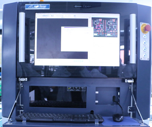
As a type of classical inspection technology in recent years, AOI (Automated Optical Inspection) has developed at such a high speed that AOI equipment has been widely applied for SMT (Surface Mount Technology) PCB (Printed Circuit Board) assembly. AOI works to capture images through a rotating camera that will automatically scan PCB and then comparison will be made between tested solder joints and eligible parameters in database. Image processing will lead defects on surface mount PCBs to be exposed and those defects will be displayed or indicated through monitor or automatic marker so that rework staff will be able to work on them.

AOI is mainly responsible for the following inspection goals.
a. End Quality, namely the inspection implemented for products' status before they leave manufacturing line. This inspection goal should go first when manufacturing issues are clear, SMT PCB assembly covers a high mix, and quantity and speed should be critically considered. Under such condition, AOI equipment is usually placed at the end of assembly line where it is capable of generating a large amount of process control information on a large scale.
b. Process Tracking, namely the process during which AOI equipment is leveraged to monitor surface mount assembly process typically in terms of detailed defect classification and component mounting displacement information. Manufacturers should first take advantage of this goal when products' reliability matters, high volume low mix assembly is in need and components supply falls into a stable situation. As soon as this goal is determined, AOI equipment should be placed on several places along surface mount assembly line so that specific manufacturing situation can be monitored on line and necessary basis will be provided to manufacturing technique adjustment.
Although AOI equipment can be placed at multiple positions along manufacturing line and its placement on each position will lead to different defects inspection, AOI equipment should be placed at a position where most defects can be recognized and corrected. Three inspection positions can be considered:
a. After Solder Paste Printing. If solder paste printing process totally conforms to requirement, defect count inspected during ICT (in-circuit test) will dramatically go down. Typical solder paste printing defects include:
• Insufficient solder paste on pad
• Excessive solder paste on pad
• Mismatching between solder paste and pad
• Solder bridging between pads
In the process of ICT, probability of defects mentioned above is relatively proportional to severity of issues. Slightly insufficient solder paste will seldom lead to defects while absence of solder paste, however, will almost lead to defects during ICT. Insufficient solder paste may be one of the reasons leading to missing components or open circuits. Nevertheless, missing components are caused by other reasons, which is the premise to determine where to place AOI equipment. Moreover, those reasons have to be contained into inspection schedule. Specific placement inspection directly supports process tracking and characterization. During this stage, quantitative process control data includes printing displacement and solder paste volume and qualitative information on printing solder paste will be generated as well.
b. Before Reflow Soldering. When AOI equipment is placed before reflow soldering, automated optical inspection is implemented after solder paste printing and before reflow soldering, which is a typical inspection position for AOI because this position is able to make most defects exposed deriving from solder paste printing and component mounting. The quantitative process control information generated at this position provides alignment information about IC mounter and fine pitch component mounter that can be used to modify component mounting or calibrate surface mounter. Generally speaking, this position inspection enables to meet the target of process tracking.
c. After Reflow Soldering. AOI equipment is placed after reflow soldering, that is, the final phase of surface mount assembly. This position is the most prevalent selection of AOI since full-scale assembly issues can be captured when AOI equipment is placed after reflow soldering. Automated optical inspection after reflow provides high security since it recognizes issues caused by solder paste printing, component mounting and reflow soldering.
ICT
ICT equipment is the most fundamental device applied in electrical test. The traditional ICT device takes advantage of specialized bed nail that contact with components that have been soldered solidly on PCB board and certain voltage and current are used to carry out final test so that component defects can be known including missing, displacement, misplacement, parameter deviation, solder joint bridging, opens and shorts etc. Bed nail works appropriately for simple PCBAs and mass volume production due to its high speed and low cost. However, as PCB assembly density gradually goes up, fine pitch SMT assembly and new product introduction goes through an increasingly short period and PCB boards go to diversity, bed nail test have to be confronted with some indispensible issues that fail to be overcome. It even fails to carry out test on some high-density SMT PCB assembly.
Another prevalent ICT method for SMT PCB assembly is flying probe test which depends on a large amount of flying probes to test electrical performance of circuits. Nevertheless, it is widely accepted to be applied in PCB fabrication test. As it is used in surface mount assembly test, it is able to do more.
AXI
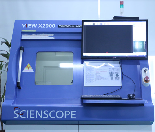
Compared with AOI, AXI is a newly-developed inspection method. As assembled PCB boards enter AXI equipment along rail, the X rays will be absorbed by the detector below after being transmitted by transmitting tube and going through PCB. Since solder joints contain so much lead that can absorb X rays, well-formed solder joints will display black dots on the image while X rays penetrating some materials such as glass fiber, copper or silicon. Therefore, X ray inspection makes solder joint so direct and clear that solder joint defects can be automatically inspected through image analysis algorithms.

Thanks to the development of modern technology, X ray inspection has developed from 2D to 3D. As an inspection method through X ray transmission, the former generates clear images of component solder joints that are placed on single-sided board while performing badly on double-sided board. The latter, however, takes advantage of layering technology so that it is capable of inspecting solder joints on double-sided board. Moreover, 3D X-ray inspection is also able to inspect defects of those unseen solder joints such as BGA solder joints and PTH solder joints. Furthermore, solder in PTH holes can be inspected to ensure its sufficiency so that solder joint quality will be dramatically improved.
Comparison between AOI, ICT and AXI
Each coin has two sides.
ICT is one of the commonest test methods applied during manufacturing process with its advantages: high defect observation capability and high test speed. ICT is accepted by companies requiring mass volume products due to its convenient and fast features. Nevertheless, when it comes to users requiring low volume and multiple types of products, it is inappropriate because bed nails need to be often changed. Plus, as circuit becomes more complex and being of more density, traditional test method has to face up with extreme limitations and it's increasingly difficult for ICT to find out defects. Furthermore, more contact points adding will tend to cause test errors and more retesting.
The biggest advantage of AOI lies in extreme short test programming time and high flexibility. Apart from defects that visual inspection fails to inspect, AOI is also capable of accumulating manufacturing quality of each link and defect types that will be provided to technology control engineers for analysis and management. Disadvantages of AOI include failure to detect circuit errors and disability to detect unseen solder joints.
As a relatively mature inspection technology, AXI is capable of covering manufacturing defect rate as high as 97% and inspecting solder joints that cannot be seen with naked eyes. Nevertheless, AXI fails to test defects in terms of electrical performance.
Learn to make best of them.
Now that each inspection method features its own advantages and disadvantages, they are not actually either/or relationship while they complement to each other. ICT, AOI and AXI can be first classified into two categories: ICT and AOI/AXI since ICT is responsible for inspecting defects in circuit while AOI/AXI is for appearance defects. In conclusion, ICT should be definitely picked up and either AOI/AXI or their combination should be considered.
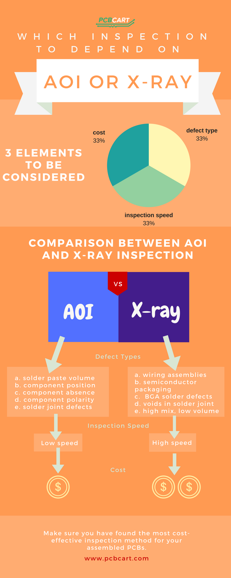
AOI/AXI plays a significant role in determining surface mount assembly quality. They differ from each other in lots of aspects:

Based on the depiction in the above image, cost, defect type and inspection speed are mainly elements that should be taken into consideration when you are ready to pick up an ideal inspection method for surface mount PCB.
PCBCart Has The Capabilities to Carry Out AOI, ICT and AXI on PCBs
PCBCart has been printing PCBs for electronic manufacturers for over twenty years. We can provide AOI, ICT and AXI to meet different demands. If you are having PCB production demands and interested in getting more details on our PCB inspection capabilities, please check following pages:
• PCBCart Performs 100% Electrical Test on Each Piece of PCB Boards
• FREE Automated Optical Inspection Option from PCBCart
• Automated X-ray Inspection from PCBCart
• Here is Why You Should Let PCBCart Manufacture Your PCBs
It is crucial to go through the complicated world of PCB SMT assembly with appropriate selection of inspection technology to ensure quality and efficiency. The foregoing article has presented a comparative view of AOI, ICT, and AXI, which are different in terms of capabilities and limitations. AOI excels at its speed and rapid defect detection, ICT excels in high-volume production with its thorough electrical testing, and AXI gives thorough information about hidden solder joints to give thorough quality.
With the effective integration of these technologies, manufacturers can maximize their inspection process and give optimal results. Contact PCBCart for a quote today, and have our experts leverage the latest inspection technologies to ensure the optimal quality and performance of your PCB SMT assembly.


