With the development of chip packaging technology, BGA (ball grid array) has been regarded as a standard packaging form. As far as chips with hundreds of pins are concerned, the application of BGA package brings forward tremendous advantages.
BGA chips win over QFP (quad flat package) chips in terms of the shape of BGA packages. BGA packages make the physical size of chips dramatically reduced with solder ball array replacing peripheral leads at QFP chips, which is especially obvious when multiple I/O pins are available. The surface area of BGA linearly increases with the improvement of I/O pin count while that of QFP increases with the improvement of I/O pin count square. As a result, BGA package provides more manufacturability to components with multiple pins than QFP. Generally speaking, I/O pin count ranges from 250 to 1089, which is specifically determined by packaging type and size. As far as manufacturability is concerned, BGA chips also perform better than QFP chips. The pins of BGA package chips are ball-shaped and are distributed in 2D array. Moreover, I/O pins feature larger pitch than QFP and perform as hard balls that won't be deformed due to contact. When it comes to chip manufacturers, another merit of BGA chips lies in its high yield. The assembly defect rate of BGA chips is normally at 0.3ppm to 5ppm per pin that can be regarded as equivalently no defect.
Thanks to the reasons discussed above, BGA package chips are widely applied by electronic assemblers. However, the peculiar shape of BGA packages leads to higher risk of short circuits in soldering unless some important layout tips are leveraged in the design phase. Thus, this article will in the remaining part demonstrate some important layout rules for BGA chips so that optimal soldering effect can be obtained in SMT (surface mount technology) assembly.
• Pitch and Spacing
Solder ball pitch for BGA packages generally remains at 50mil. To meet the requirement of technology used in PCB (printed circuit board) manufacturing process, the spacing between through hole and pad edge should be at least 8mil and the spacing between traces and pad edge can be reduced to 5mil to 6mil. Therefore, it's reasonable to define pad size of BGA chips to be between 18mil to 25mil and tracing width between BGA solder balls should be in the range from 6mil to 8mil.
• Positioning Mark Setting
Because BGA packages are hardly inspected by naked eyes and solder joints even fail to be seen by naked eyes, accurately fiducial marks should be set to be compatible with the requirement of assembly inspection, manual assembly and replacement after rework.
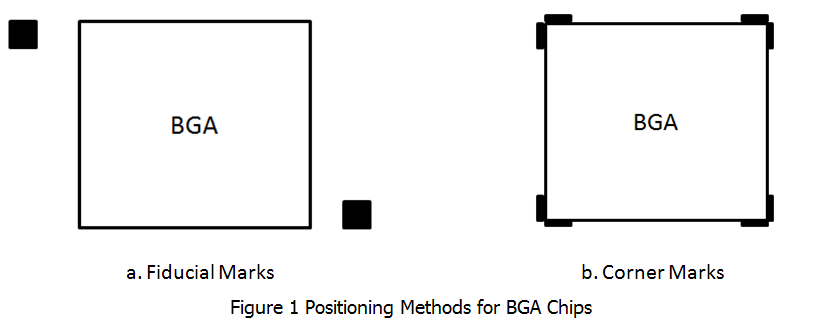
It's a usual practice to place either two fiducial marks at opposite corners of a BGA component or two corner marks, as is depicted in the following figure.

Both fiducial marks and corner marks are placed at the equivalent layer with BGA packages, that is, component layer. Fiducial marks ordinarily feature three types of shape: square, circle and triangle whose size ranges from 20mil to 80mil with an area without solder mask covered remained with a size of 60mil. The width of corner marks is in the range from 8mil to 10mil, providing the most accurate alignment for BGA pad graphics.
• Conductive Through Holes between Pads
Generally speaking, through holes should NOT be arranged between pads with blind vias and buried vias replaced. Nevertheless, that method will lead to a higher cost for PCB fabrication. If through holes have to be applied between pads, solder mask oil should be used to stop solder from flowing off or to get holes filled or covered to stop short circuits in soldering.
• Pad
Among all the pins of BGA chips, there are a lot deriving from power or ground. If a pad is designed as a through hole, lots of space will be saved for tracing. However, this type of design only works for reflow soldering technology. As through hole assembly method is used, through hole volume should be compatible with the amount of solder paste. As long as that technology is applied, solder paste will get through hole filled. With that element out of consideration, solder balls will sink into solder joints with conductivity going down.
BGA chip layout is never limited within the above aspects and it's almost impossible for a single article to cover all the layout tips for BGA chips. Apart from the above items, BGA component layout is also associated with the capabilities and equipment parameters of contract manufacturers or assemblers. For example, the maximum and minimum board size a chip mounter is capable of dealing with might differ from each other, calling for corresponding design modifications to be compatible with different design requirement. As a result, it's of great significance to make full confirmations about everything concerning BGA chip layout to obtain optimal performance of assembled PCB and further final products.
PCBCart Offers All-Around BGA Component Layout Suggestions for Your Optimal Balance Achievement between Cost and Functions
Prior to real manufacturing or assembly, times of confirmations are needed by engineers from PCBCart. That is totally worthwhile actually. All the confirmations go for perfect matching between your design, our manufacturing capabilities and our equipment parameters and for the largest extent of time and money saving with no expected functions compromised. Want BGA component layout suggestions right now? Note: they are FREE. Try an online quote by clicking below button. We will calculate your custom PCB Assembly cost.
Request for FREE BGA SMT Assembly Quote
Helpful Resources
• An Introduction of BGA Packaging Technology
• Factors Affecting the Quality of BGA Assembly
• Application of Surface Mount Technology (SMT) on Ball Grid Array (BGA) Packages
• Effective Measures for Quality Control on Ball Grid Array (BGA) Solder Joints
• Requirements on Design Files to Ensure Efficient BGA Assembly
• How to Get Precise Quote for Your BGA Assembly Demands


