



For BGA and fine-pitch assembly, choose a flat finish. ENIG is the sensible default for most boards, ENEPIG earns its higher price when the board also carries wire-bonded die or will go through many thermal cycles, and immersion silver or OSP work well when cost or high-frequency loss matters more than shelf life. HASL is the finish we steer people away from, because its uneven solder crown works against both stencil printing and ball placement on small pads.
In our experience the chemistry matters less than two practical questions: how many reflow passes will the board see, and how long will bare boards sit before they reach the SMT line? Answer those honestly and the choice usually makes itself.
Why does surface finish matter more at fine pitch?
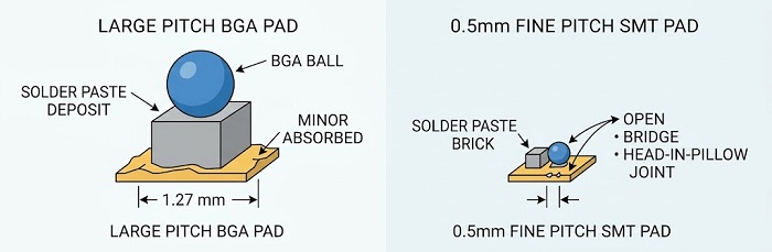
Because the solder volume shrinks while the variation in the finish does not. On a 1.27 mm pitch BGA, a pad that sits a few microns high or carries a little oxidation gets absorbed by a generous paste deposit and a large ball. At 0.5 mm pitch and below, the aperture is small, the paste brick is small and the ball is small, so the same variation turns into an open, a bridge or a head-in-pillow joint.
Four properties of the finish feed straight into assembly yield on these parts:
• Planarity. The stencil has to gasket flat against each pad. A domed or uneven pad lets paste squeeze out under the foil or leaves a short deposit.
• Wetting. Small pads give solder very little area and time to spread. A finish that wets slowly leaves partially wetted pads that nobody can see once the package is down.
• Condition after the first reflow. On a double-sided board, the second side is printed onto pads that have already seen one peak temperature. Some finishes come through that well; others lose a good share of their solderability.
• The interface left behind. The finish decides whether the joint forms on copper or on nickel, and that interface is where BGA joints usually fail under drop, bending or thermal cycling.
None of this shows up on an AOI image of a BGA, because the joints are hidden under the package. X-ray finds bridges and large voids, but it will not tell you that a joint is sitting on a weak interface. That is why we treat finish selection as part of BGA assembly planning at the quoting stage rather than a box ticked on the fab order.
For reference, our standard FR4 boards support a minimum BGA/SMD spacing of 0.2 mm. At that end of the range every one of the properties above is working close to its limit, and it is worth checking your parts against our list of supported SMT packages before the finish is locked in.
Why is HASL a poor fit for BGA and fine-pitch parts?
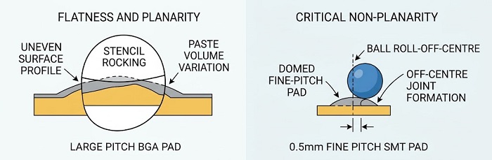
Because it is the least flat finish on the menu. HASL dips the panel in molten solder and strips the excess with hot air knives. The coating that remains varies with pad size, pad orientation relative to the knives and position on the panel. Small pads tend to come out with a rounded crown, while large pads end up flatter.
On a BGA land pattern that crown causes three separate problems. The stencil rocks on the high points and does not seal, so paste volume changes from pad to pad. Balls can roll off-centre during placement, which is more noticeable on light CSPs. And the solder already on the pad adds to the joint volume in a way your stencil design never accounted for.
Lead-free HASL adds a thermal penalty on top. The solder pot runs hotter than it did with tin-lead, so the bare board takes an extra high-temperature excursion before assembly has even started. On a thick multilayer board, that is one more round of z-axis expansion through every plated hole.
HASL and lead-free HASL are still reasonable for boards dominated by through-hole parts and coarse SMT, and we supply both. The catch is that the finish covers the whole board. If one fine-pitch BGA sits in a corner, that BGA should decide the finish, not the rows of through-hole connectors around it.
ENIG: where it works and the black pad question
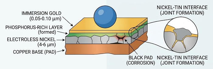
ENIG is the finish we suggest for most BGA boards, provided the plating line is well controlled. It lays down several microns of electroless nickel-phosphorus followed by a thin immersion gold layer, with thickness requirements set out in IPC-4552. The result is flat, keeps well in storage and handles multiple lead-free reflow passes without the solderability loss you see on organic or tin-based finishes.
During soldering, the thin gold dissolves into the solder almost immediately and the joint actually forms on the nickel. That nickel-tin interface is the part that carries the load, and it is also where ENIG’s known weakness lives.
Black pad is corrosion of the nickel that happens in the immersion gold bath. Immersion gold is a displacement reaction, meaning gold deposits by dissolving nickel. When that attack goes too far, usually through bath chemistry drift, excessive dwell time or nickel with the wrong phosphorus content, the nickel grain boundaries corrode and a phosphorus-rich layer forms under the gold. The board looks normal. Solder may even wet acceptably. But the joint sits on a weakened layer and can fracture cleanly along it under mechanical shock or board flexing.
What makes black pad frustrating is that routine inspection will not catch it. AOI and X-ray see nothing unusual. Finding it takes cross-sectioning, stripping the gold and looking at the nickel surface under SEM, or destructive pull and shear tests on sample joints.
This is a process-control problem, not a reason to abandon ENIG. The controls that matter sit on the plating line: bath pH, stabilizer and metal concentrations, nickel phosphorus content and gold immersion time. If your product will be dropped, vibrated or flexed in service, tell us at the quoting stage, so qualification testing can be agreed with our engineering team before the design goes to volume.
Two smaller points engineers sometimes miss. ENIG accepts aluminium wire bonds but is not a dependable surface for gold wire bonding. And solder does not always spread to the very edge of an ENIG pad, which can look odd on QFN side fillets but is normally acceptable when the joint meets IPC-A-610 criteria.
When is ENEPIG worth the extra cost?
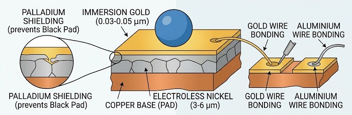
ENEPIG pays for itself when the board needs something ENIG cannot give: dependable gold wire bonding, lower black pad exposure on a product with strict drop or vibration requirements, or soldering and bonding on the same surface. For a typical industrial controller with a few BGAs and one or two reflow passes, it rarely adds enough to justify the price.
The stack adds a thin electroless palladium layer between the nickel and the gold, with requirements defined in IPC-4556. Palladium shields the nickel from the immersion gold bath, which removes most of the mechanism behind black pad. It also gives a surface that takes both gold and aluminium wire bonds, which is why ENEPIG is often called the universal finish.
These are the cases where we would usually recommend it:
• Boards that combine SMT parts with chip-on-board die or other wire-bonded devices, so that one finish serves both processes.
• Products where an interfacial BGA fracture would be expensive to discover in the field, and where the qualification plan includes drop or bend testing.
• Assemblies that will see several reflow passes plus planned BGA rework during NPI or test.
• Boards that mix soldered parts, press-fit connectors and exposed contact surfaces.
ENEPIG carries its own process risk. If the palladium layer is too thick, wetting slows and joint quality can suffer, so palladium thickness has to stay inside the specified window. Cost also moves with the palladium market, so treat the price difference against ENIG as something to quote per project, not a fixed ratio.
On RF and high-speed boards, remember that ENIG and ENEPIG both put nickel in the current path at the pad. At most frequencies the effect is small. If your loss budget is tight at microwave frequencies, raise it with us early, because the right answer may be a nickel-free finish.
Immersion silver, immersion tin and OSP: shelf life and reflow cycles
All three are flat, cost less than the gold-based finishes and form the solder joint directly on copper. The trade-off is sensitivity to time, handling and heat before assembly, which matters most on double-sided boards and staggered HMLV builds where bare boards may wait weeks for a kit to complete.
Immersion silver. A thin silver layer over copper, very flat, with good solderability and no nickel in the signal path, which makes it attractive for high-speed and RF designs. Its weak points are tarnish and sensitivity to sulfur in the air and in packaging materials. A poorly controlled process can also leave small voids at the copper-silver interface, and on a BGA those sit directly under the ball. Keep boards sealed in sulfur-free packaging and handle them with gloves. In sulfur-rich service environments, creep corrosion is a known risk on uncoated assemblies.
Immersion tin. Flat and well suited to press-fit pins. The problem for BGA work is that copper and tin form an intermetallic that keeps growing at room temperature and grows faster with each heat cycle, eating the free tin the solder needs. A board that wets well on the first side can wet noticeably worse on the second. Tin whiskers are another consideration for long-life products. We offer immersion tin, but we rarely suggest it for double-sided BGA boards.
OSP. A thin organic film that keeps copper clean until soldering. It is flat and usually the lowest-cost option, and joints formed directly on copper hold up well in drop testing. The film degrades with every thermal exposure, though. After the first reflow, pads waiting for the second side carry a thinner, partly broken-down coating, and their wetting depends on how soon the second pass follows and whether the oven runs nitrogen. OSP boards should not be baked to remove moisture, since baking degrades the coating. Unsoldered test pads also stay covered by a non-conductive film, which can make in-circuit test probing unreliable.
The table below puts the six finishes side by side from an assembly point of view.
| Finish | Planarity | Typical sealed shelf life* | Reflow tolerance* | Joint forms on | Main assembly risk |
|---|---|---|---|---|---|
| HASL / lead-free HASL | Poor | Around 12 months | Good | Copper (via solder coat) | Domed pads, extra thermal cycle |
| ENIG | Excellent | Around 12 months | Multiple passes | Nickel | Black pad, interfacial fracture |
| ENEPIG | Excellent | Around 12 months | Multiple passes | Nickel | Palladium thickness control, cost |
| Immersion silver | Excellent | About 6–12 months | Several passes | Copper | Tarnish, sulfur, interfacial microvoids |
| Immersion tin | Excellent | About 6 months | Degrades each pass | Copper | IMC growth, whiskers |
| OSP | Excellent | About 6 months | Usually 2 passes; nitrogen helps | Copper | Film breakdown, no baking, ICT probing |
*Shelf life and reflow figures are general industry guidance, not commitments from us. Actual values depend on chemistry, packaging, storage temperature and humidity, so confirm them with our engineering team for each project.
Decision table by package and process
Pick the finish for the most demanding package and the most demanding process step on the board, then check it against how long bare boards will be stored. The table below covers the situations we see most often.
| Board situation | First choice | Also workable | Avoid |
|---|---|---|---|
| QFP/QFN at 0.5 mm pitch or coarser, single reflow pass, assembly soon after fab | OSP | ENIG | HASL |
| BGA at 0.8–1.0 mm pitch, double-sided reflow | ENIG | ENEPIG, immersion silver | HASL, immersion tin |
| Fine-pitch BGA or CSP at 0.5 mm pitch or below, double-sided | ENIG | ENEPIG | HASL, OSP if second pass is delayed |
| BGA plus wire-bonded die (COB) on the same board | ENEPIG | None in practice | HASL, OSP, immersion tin |
| BGA with tight high-frequency loss budget | Immersion silver | ENEPIG (check loss) | HASL |
| Press-fit connectors plus SMT | Immersion tin or immersion silver | ENEPIG | HASL |
| Bare boards stored or kitted for staggered HMLV builds | ENIG | ENEPIG | OSP, immersion tin |
| BGA rework expected during NPI or test | ENIG or ENEPIG | Immersion silver | OSP, immersion tin |
| Mostly through-hole, no BGA, cost-driven | Lead-free HASL | OSP | — |
| In-circuit test on unsoldered test pads | ENIG | Immersion silver | OSP on test pads |
Before you release the fab drawing, run through this short checklist:
• State the finish and the IPC specification it should meet: IPC-4552 for ENIG, IPC-4556 for ENEPIG, IPC-4553 for immersion silver or IPC-4554 for immersion tin. For any thickness tighter than the specification, confirm with our engineering team.
• Tell us how many reflow passes the board needs and whether BGA rework is planned.
• If boards will be stored or kitted for later builds, write down the expected storage time so the finish matches it.
• If ICT is planned, check which test pads stay unsoldered and what finish they will carry.
• Flag wire-bonded die and press-fit parts, so the finish serves those processes as well as soldering.
Getting the finish right with PCBCart
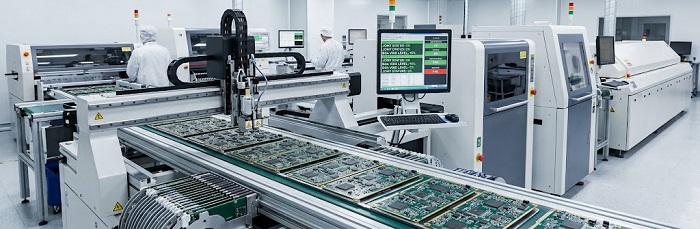
At PCBCart we build boards from your Gerber data and assemble them in the same program, so the finish decision and the assembly process get reviewed together instead of being handed across a supplier boundary. On standard FR4 we offer HASL, lead-free HASL, ENIG, ENEPIG, immersion silver, immersion tin and OSP, and during DFM review our engineers check the finish against your package mix, reflow sequence and planned storage time. Production runs in our Hangzhou and Thailand factories, and high-mix, low-volume builds with BGA and fine-pitch parts are a regular part of that work. Send us your Gerbers and BOM, tell us how the board will be built and stored, and we will tell you which finish we would use and why.
FAQ
Can I use two different finishes on one board?
Yes, selective combinations exist. The common one is ENIG on SMT pads with hard gold on edge-connector fingers; ENIG on some areas with OSP elsewhere is another. Each combination adds masking steps and cost, and not every pairing suits every panel layout. Whether a specific combination works for your design is something to confirm with our engineering team before the drawing is final.
Does surface finish change BGA void levels?
It plays a smaller role than paste chemistry, reflow profile and pad design, with via-in-pad being the usual suspect. Where finish does show up is in interfacial microvoiding, which has been associated with immersion silver run outside its process window. If voiding is a qualification criterion, agree the acceptance limit and X-ray sampling plan with our engineering team rather than relying on finish choice to control it.
Does the finish matter if a BGA has to be reworked?
Yes. Rework heats the site and partly heats its neighbours, so pads on OSP or immersion tin lose solderability with each cycle, both at the reworked site and around it. ENIG and ENEPIG tolerate repeated local heating much better. If your NPI plan expects BGA swaps during debug or test, that alone is a good reason to choose a gold-based finish.
Can black pad be caught on incoming bare boards?
Not by visual inspection or electrical test. Solderability testing to J-STD-003 on coupons will catch gross problems but not every case. The dependable methods are destructive: cross-section, gold stripping and SEM inspection of the nickel. If your program needs lot-level evidence, confirm with our engineering team what testing and records can be provided for your order.
Is ENEPIG automatically the safer choice for life-science or semiconductor test boards?
No. The process decides, not the sector label. An ATE interface board with many fine-pitch BGAs, repeated rework and long service life often justifies ENEPIG or a tightly controlled ENIG. A diagnostic instrument board assembled in a single pass and shipped soon after fab is usually well served by ENIG.
Helpful Resources


