SMT (Surface Mount Technology) assembly has become a leading electronics manufacturing technology as far as performance and efficiency are concerned by electronics products. With high reliability guaranteed, low cost can be definitely regarded as the secondary key element that has to be considered by OEMs (Original Equipment Manufacturers).
SMT assembly procedure consists of so many steps each of which contributes to the quality of final products. Furthermore, any modification occurring to each manufacturing step may possibly cause a huge cost fluctuation. Therefore, it’s substantially positive to have a full understanding of SMT assembly procedure, which is also a shortcut to cost reduction without performance being sacrificed.
Generally speaking, SMT assembly procedure mainly contains the following steps: solder paste printing, solder paste inspection (SPI), chip mounting, visual inspection, reflow soldering, AOI, visual inspection, ICT (In-Circuit Test), function test, depanelization etc. And, a full understanding of the whole procedure helps you to reduce production cost.
Step#1: Solder Paste Printing
SMT assembly starts from solder paste printing that aims to place a proper amount of solder paste onto pad on which components will be soldered. The quality of solder paste printing is mainly determined by three elements: solder paste condition, scraping angle and scraping speed.
High quality can never be obtained by SMT assembled PCBs unless solder paste is properly stored and applied. Solder paste has to be stored in a fridge to be kept in a low temperature and its temperature should be recovered to room temperature prior to its application on SMT manufacturing line. Moreover, the uncovered solder paste has to be used up in two hours. Apart from solder paste status, solder paste printer parameters should be properly set, which is especially true for scraping angle and speed since both parties are closely related with the specific amount left on pad.
Step#2: Solder Paste Inspection (SPI)
Solder paste inspection in itself is an optional way to reduce cost because it’s better to reduce solder defects right now than to catch them later. SPI is not a must-be step in SMT assembly procedure but with it applied it’s beneficial to decrease your manufacturing cost and to improve the quality of products. After all, most defects in SMT assembly derive from solder paste printing and if they can be found out and dealt in the early phase, the threats possibly leading to defects in later stages of manufacturing will be decreased or even eliminated. SPI machine features two types: 2D and 3D. PCBCart owns a 3D SPI machine in the workhouse to provide better inspection service to customers.
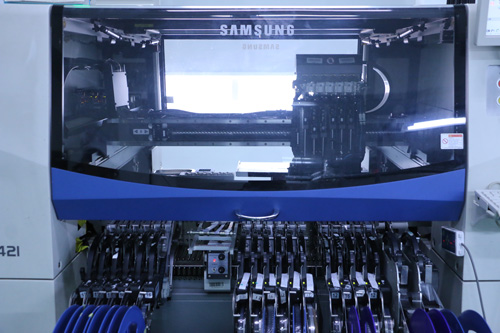
Step#3: Chip Mounting
Chip mounting plays a core role in SMT assembly process. Chip mounting is completed by chip mounters that differ from each other primarily in terms of speed and mounting capability. Some small components are normally placed by high-speed chip mounters that are capable of placing them quickly to make those components quickly adhered to the solder paste on pad.
However, big components such as BGAs, ICs, connectors, etc. are usually placed by multi-function chip mounters that run at a relatively low speed. As far as those components are concerned, alignment does matter. It takes more time to achieve alignment prior to chip mounting, which is why the speed of multi-function chip mounter is much lower than that of high-speed chip mounter. Moreover, some of the components used in multi-function chip mounter don’t rely on tape on reel while some on tray or tube due to the limitations of size.
Step#4: Visual Inspection + Components Placement by Hand
After chip mounting, it’s necessary to carry out visual inspection so that reflow soldering can be largely ensured to be without defects. The leading issues to be found out in this step include misplacement, missing parts, etc. The defects are extremely difficult to be dealt with once reflow soldering is done because they will be solidly fixed onto PCB. As a result, products’ reliability will go down and production cost will rise as well.
On the other hand, some components can be placed directly by hand in this step, including some large components, DIP components or those that can’t be placed through chip mounter due to some reasons.
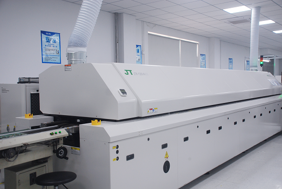
Step#5: Reflow Soldering
In the process of reflow soldering, solder paste is melted to generate IMC (Intermetallic Compound) to connect component pins and board. The temperature profile followed in the process of reflow soldering process covers preheating, temperature rise, reflow and cooling. Take lead-free solder paste SAC305 as an example, its melting point is approximately 217℃ so the solder paste can’t be remelted unless the temperature of reflow soldering oven is higher than 217℃. Furthermore, the highest temperature of reflow soldering oven shouldn’t be higher than 250℃, or a lot of components can’t be melted due to their incapability to withstand such a high temperature.
As a matter of fact, temperature profile setting determines reflow soldering quality and helps reducing production cost. Thus, it’s better to find out experienced SMT assembler as a CM (Contract Manufacturer) who is fully aware of elements influencing SMT soldering quality and improvement measures. All the elements will lead production cost to be cut.
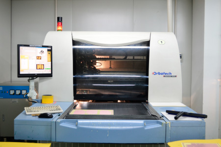
Step#6: AOI (Automated Optical Inspection)
Up to now, components have been fixed onto PCB after reflow soldering, which means that the essential part of task concerning SMT assembly has been completed. However, the assembled boards can never be directly used in final products unless sufficient test and inspection have been made. Performance of solder joints can be inspected through the application of AOI that is capable of exposing some defects like tombstone, edge on, missing components, misplacement, orientation, bridging, empty solder etc.
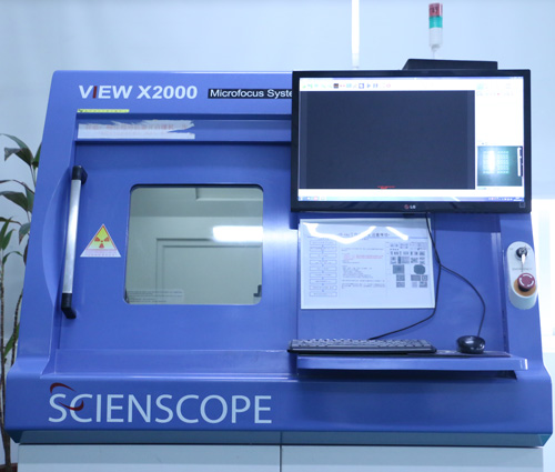
Step#7: AXI (Automated X-ray Inspection)
X-ray inspection is a supplement to AOI since it is capable of indicating some defects more clearly and directly. It’s not a must-be measure after reflow soldering. However, as long as the SMT assembler cares more about products’ quality and reliability, X-ray inspection machine will be definitely applied to meet the rigorous demands of some OEMs for the achievemtn of higher efficiency.
Step#8: ICT or Function Test
The aim of ICT is to test whether opens and shorts are available in the circuit and to expose some defects of some components by measuring resistance, capacitance and inductance. As a result, components are tested to ensure their high performance after reflow soldering.
Function test is a supplement of ICT since ICT can only test the opens and shorts on bare board but the functions of assembled PCBs fail to be tested. Therefore, the functions of assembled PCBs should be tested through function test in order to maintain the high reliability of final products.
Now Up to $800 Discount Waiting for YOU
Helpful resources:
• PCB Assembly Service
• Prototype PCB Assembly Service
• Low-Volume PCB Assembly (HMLV) Service
• High Volume PCB Assembly Service
• Full Turnkey PCB Assembly Service