Lead-free PCBs (Printed Circuit Boards) were first called for just for the compliance of ROHS (Restriction Of Hazardous Substances) by EU (Europe Union) that requires all the electronics have to conform to ROHS regulations. As a result, PCB fabrication starts to convert from lead to lead-free.
The lead in solder joints mainly derives from plated pins of components, PCB plated pad and solder. To ensure the lead content in solder joints conforms to ROHS regulations (mass fraction should be lower than 0.1%), surface finish applied on PCBs, therefore, has to be lead-free compatible. Right now, a couple of surface finishes have been generated for the achievement of lead-free fabrication and ENIG, ImAg, ImSn and OSP are most widely applied.
Since each type of surface finish features its own advantages and disadvantages, it’s important to be clear which type of surface finish is optimal as far as your projects are concerned. Thus, this article will compare the four types of surface finishes primarily based on the analysis on application condition, cost, compatibility with lead-free requirement, shelf life, solderability etc. so that you’ll be able to figure out the optimal surface finish for your lead-free PCBs.
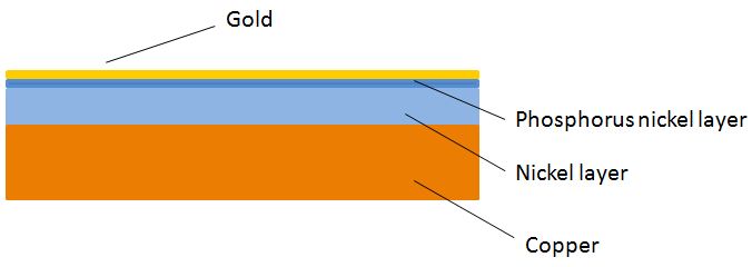
ENIG
ENIG is short for Electroless Nickel/Immersion Gold and its structure is displayed below.
• General Description
As a lead-free surface finish, ENIG features some obvious ADVANTAGES, including long storage time, excellent solderability and flat surface. Its key DISADVANTAGE lies in relatively high cost and “black pad” risk.
• Black Pad
Black pad is actually a defect occurring to soldering joints with ENIG applied, which results from the fact that nickel layer suffers from severe erosion. Because the broken nickel layer looks grey and black, it is called black pad.
The leading disadvantage of black pad lies in the fact that it is difficult to be eliminated. Furthermore, it can’t be inspected by naked eyes. Therefore, it adds more threat to products’ reliability.
• Disadvantage Discussion
a. Non-wettability
Non-wettability is the direct cause of black pad. Generally speaking, the ENIG-coating PCB suffering from black pad fails to withstand stress effect. As a result, once products go through high-low temperature cycle test, vibration test and daily plug in and out, solder joints will suffer from fraction, reducing products’ reliability.
b. Tendency to Errosion
Solder joints with ENIG applied tend to become eroded in humidity more easily because gold layer is so thin and features pinholes. Gold, however, doesn’t become eroded and it’s the nickel layer beneath gold layer suffers from erosion.
• Summary
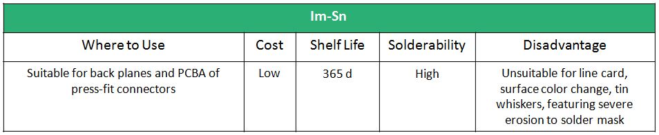
Im-Sn
Im-Sn is a short form of immersion tin that is achieved through replacement reaction to form a pure tin layer on the surface of copper. Due to replacement reaction, the thickness of surface finish is limited, which is normally 1μm.
• Disadvantage Discussion
a. Non-resistant to Storage
Even in normal temperature, tin layer and copper matrix tend to be diffused to each other. Under room temperature, the diffusion speed of tin remains approximately in the range from 0.144 to 0.166nm/s and it can be stored under room temperature for 30 days. And, tin thickness will be lost by 0.23μm to be converted into IMC. After reflow soldering, its thickness will be reduced by more than 0.8μm. When it needs being stored for 180 days, soldering has to be implemented for three times. The minimum thickness of Im-Sn has to be over 1.28μm. However, that usually fails to be done and the ordinary thickness is just 1.15μm.
b. Color Changing
As temperature constantly goes up in the process of soldering, Im-Sn layer tends to change color, resulting from organic pollutants or tin dioxidation. Generally speaking, the thicker tin dioxide becomes, the deeper its color will be.
c. Not Fit for Fine Pitch Assembly
Because tin plating chemical solution arouses bad effect on most solder mask, solder mask can’t be too small. Or, it will be broken. Therefore, Im-Sn doesn’t work on fine-pitch assembly.
d. Tin Whiskers
Tin whiskers are for Im-Sn as black pad for ENIG. Tin whiskers usually occur to Im-Sn and spacing between pads can be set to be more than 0.4mm.
e. Solution Attack
Due to the attck from chemical solution, via-filled ink tends to suffer from fractions which often hide some solution that will be squeezed out during reflow soldering, badly reducing appearance and reliability.
• Summary
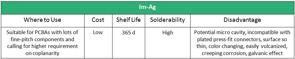
Im-Ag
Im-Ag is a short form of immersion silver that aims to generate a silver layer due to the effect of solution. Instead of a pure silver layer, Im-Ag contains organic substance whose mass fraction is approximately 30%.
• Disadvantage Discussion
a. Micro Cavity
Micro cavities whose diameter is less than 0.05mm tend to be caused on silver surface. The cavities will dramatically decrease the strength of soldering joint, which is especially obvious when PCB suffers from shock. As a result, end products may become even failed.
b. Creeping Erosion
Creeping erosion is a leading defect as far as Im-Ag is applied as a surface finish. Because galvanic coupling is caused by the combination of exposed copper at the edge of solder mask and mass-area silver surface, electrochemical corrosion tends to be generated in humidity.
c. Silver Migration
Silver migration usually occurs to thick-film circuits or interior IC.
d. Color Changing
The color of surface of board coated with immersion silver surface tends to become yellow or black after being exposed by the air. Color changing takes place in the air mainly because small holes are available on the surface of silver and color changing takes place once haloid in the air reacts with the silver holes.
Besides such cause of color changing, sometimes surface color changes after soldering. There are two elements leading to after-soldering color changing: plating thickness and exposure time. It’s been testified that the increase of plating thickness is beneficial to color-changing resistance improvement and shortening of exposure time is also capable of relatively stopping surface color from changing.
• Summary
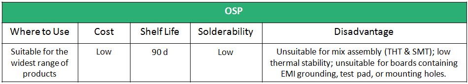
OSP
OSP is short for Organic Solderability Preservatives. OSP is actually a layer of organic film generated on clean copper surface in a chemical way. It is used to protect copper surface from being oxidized. Besides, it can resist thermal shock and wettability.
• Challenges OSP will Go Through after Soldering
Challenge#1
Under the high temperature of reflow soldering oven, volatilization hardly takes place so that mass is lost by no less than 10%, which indicates that the smallest thickness can be used on OSP.
Challenge#2
OSP won’t be decomposed under the temperature of 260℃. In the process, OSP is converted from solid directly to gas with no heat generated.
Challenge#3
OSP tends to react with oxygen in the process of soldering.
Challenge#4
As soon as OSP enters soldering oven, it’s easy for it to become rust color with its solderability deteriorated.
Challenge#5
OSP tends to become hard to be eliminated with flux applied so that stronger flux should be used instead.
• Summary
PCBCart Ready to Help YOU with PCB Solutions Online
PCBCart provides you one-stop PCB solution including PCB fabrication, PCB assembly and components sourcing. You’ll get your PCBs manufactured with top quality and bottom prices. Click the following button to start your project with a high-quality PCB.
Top-quality and Bottom-price PCB Fabrication