



High-current power module PCBA assembly carries a solder joint risk profile that standard SMT inspection routines aren't built to catch in full. Surface-level defects are visible to optical systems, but the failure modes that matter most for sustained current-carrying joints — internal voiding, incomplete thermal via fill — sit entirely below what any camera-based system can see. A combined 3D AOI and X-ray strategy, sequenced correctly and tied into batch-level traceability, closes that gap without inflating inspection time on every unit.
The Dual-Risk Profile of High-Current Power Module Solder Joints
High-current power modules — DC-DC converters, gate driver stages, power inductors and their associated MOSFET/IGBT packages in stationary industrial and grid-scale energy storage equipment — present a solder joint risk profile that differs meaningfully from fine-pitch digital assemblies.
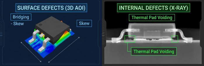
Surface-visible risks, catchable by optical inspection, include:
Solder bridging between adjacent large pads or heatsink tabs
Component misalignment/skew on large-body packages
Insufficient or excess solder volume visible at the fillet
Tombstoning on two-terminal power passives
Internally hidden risks, invisible to any camera-based system, include:
Voiding beneath exposed pad/thermal pad packages (QFN, D2PAK, power SOIC), where trapped gas during reflow prevents full wetting to the copper
Incomplete solder fill in thermal or power vias beneath the die-attach pad, which compromises the intended heat path even when the top-side joint looks acceptable
Subsurface bridging under gull-wing or J-lead terminations that overhang the visible fillet
The core inspection problem for power module assemblies is that a joint can pass visual and optical scrutiny entirely while carrying a thermal defect that only manifests as a field failure under sustained current load. This is the rationale for pairing 3D AOI with X-ray rather than relying on either technique alone.
3D AOI Limitations on Large-Pad Power Devices
3D AOI systems verify solder joint geometry — height, volume, and coplanarity — using structured light or laser triangulation. On fine-pitch components this works reliably because pad geometry is small and consistent. Large-pad power devices introduce two specific complications:
Specular reflection from large solder surfaces. Wide fillets on heavy-gauge terminals and thermal pads reflect structured light unevenly, which can register as a false height reading or false-call a joint that is geometrically sound.
High paste-volume ambiguity. Power device pads are stenciled with substantially more paste than fine-pitch pads. 3D AOI algorithms calibrated for standard SMT can flag legitimate high-volume fillets as excess-solder defects, generating false-positive rates that erode confidence in the AOI gate if thresholds aren't re-tuned per package family.
The practical mitigation is package-specific AOI programming: separate inspection algorithms and acceptance windows for power device footprints rather than applying a single fillet-height/volume standard across the whole board. This keeps AOI useful as a first-pass surface screen without generating so many false calls that operators start overriding it.
X-Ray Parameter Adjustments for Heavy Copper and Large-Pad Assemblies
Offline X-ray inspection — used here for BGA/QFN voiding analysis with oblique-angle capability — requires different exposure settings on heavy copper power boards than on standard multilayer logic boards. The general engineering relationship is illustrative rather than a fixed recipe, since actual settings depend on copper weight, board thickness, and package construction:
Tube voltage (kV): Higher copper weights (2oz+) and thicker thermal pads attenuate X-rays more than standard 1oz traces, so voltage typically needs to be raised to maintain image contrast through the additional copper mass. Under-voltage settings tuned for thin-copper boards will underexpose the image and can mask genuine voids.
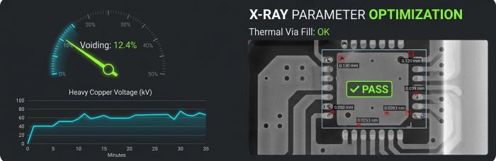
Tube current (mA) and exposure time: Larger exposed pad areas benefit from adjusted current/time combinations to resolve void boundaries clearly against the surrounding solder, particularly when correlating void percentage against IPC-A-610 acceptance criteria for thermal/exposed pad packages.
Oblique-angle imaging becomes more important on power modules than on standard BGAs, since it lets the inspector distinguish top-side voiding from voiding at the board-side interface — a distinction that matters for thermal via fill assessment specifically.
None of this implies calibration-grade metrology accreditation; the X-ray system is a manufacturing-record inspection tool, and parameter adjustments are documented as part of the inspection program rather than represented as a certified measurement process.
Inspection Sequencing: AOI First, X-Ray Confirmation Second
Running both inspection methods on every unit at full depth is inefficient. A sequenced approach reduces redundant inspection time while preserving coverage:
3D SPI verifies paste deposition immediately after printing, catching volume and registration issues before components are placed.
3D AOI, post-reflow, screens for the surface-visible defect set — bridging, skew, gross solder volume deviation — across 100% of assembled boards.
X-ray inspection is then applied selectively to power device locations and thermal pad packages, informed by AOI pass/fail data and any process flags from that reflow cycle, rather than blanket X-raying every unit at every location.

This sequencing means X-ray time — inherently slower per unit than optical inspection — is concentrated where it adds information AOI cannot provide, rather than duplicating checks AOI has already cleared. For high-mix, low-volume production runs, this is a meaningful lead-time consideration compared to full X-ray coverage on every board.
MES Traceability and Batch-Level Field Failure Correlation
Both inspection datasets are only as useful as their ability to be retrieved later. Binding AOI and X-ray results to the Smart MES UID traceability system, with laser-marked unit identifiers, means:
Each power module's AOI pass/fail record and X-ray void percentage are tied to a specific reflow oven cycle (JTR-1200D-N profile log), stencil/print batch, and inspection timestamp
If a field failure is reported on a deployed power module, the batch-level record can be pulled to check whether the unit's original void percentage was within acceptance criteria, and whether any process anomalies were flagged in the same production batch
This supports root-cause investigation without requiring destructive re-inspection of the failed unit — the original inspection data is already on file
This traceability structure is a process capability, not a certification claim; it documents what was measured and when, which is the practical value for failure correlation.
Designing an Inspection Strategy for Power Module PCBA
For high-current power module PCBA, an inspection strategy should be built around three design points:
Package-specific AOI programming rather than uniform thresholds, to avoid false calls on high-volume power device fillets
Adjusted X-ray exposure settings for heavy copper and thick thermal pads, applied where voiding and via fill genuinely need confirmation
Sequenced, MES-linked inspection so surface and internal defect data are both captured, both retrievable, and neither redundantly duplicated
These are process design decisions specific to power module geometry — they aren't generic SMT inspection defaults, and treating them as such is a common source of undercaught thermal defects in power electronics assembly.
If you're scoping an inspection plan for a high-current power module PCBA program, submit your project details for a quote and our engineering team can walk through inspection strategy as part of the DFM review.
Helpful Resources
• X-Ray BGA Void Inspection for Industrial Power Modules
• Comparison of AOI, ICT and AXI and When to Use Them during PCB SMT Assembly
• Effective Measures for Quality Control on BGA Solder Joints
• Solder Ball Issues of BGA Components and How to Avoid Them


