



Heavy copper changes your design rules in two places. On the fabrication side, every extra ounce widens the minimum trace and space: a 4 oz outer layer needs at least 9/9 mil (0.23/0.23 mm) at PCBCart, and a 15 oz outer layer needs 32/40 mil (0.81/1.02 mm). On the assembly side, the extra copper acts as a heat sink, so pads tied into heavy planes reflow last and drive the whole soldering profile.
This guide walks through both, using the limits published on our heavy copper capability page. All copper weights here are finished copper, which is what those limits refer to. Where a value is not published, we say so and point you to our engineering team rather than guess.
When is heavy copper worth it?
Heavy copper is worth it when current or heat sets the limit and widening traces on a 1 oz or 2 oz board no longer fits the space you have. If routing density is the real constraint, heavier copper usually makes things worse.
Current capacity scales with conductor cross-section, which is width times thickness, but its relationship to temperature rise is not linear. Our article on current carrying capacity covers the IPC-2221 formula and why doubling the area does not double the allowable current. In practice you can often reach the cross-section you need two ways: go wide on standard copper, or go thick and keep the footprint small.
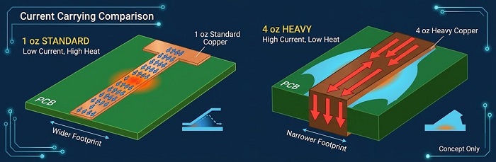
A useful first question: is the high current confined to a few nets, or does it run through a whole power section?
For a few nets, wider traces, the same net duplicated on two layers, or a mechanical busbar is often the cheaper route. When a whole section carries current, when the board has to spread heat from power devices into a plane, or when connector sites need stronger copper, heavy copper starts to pay for itself.
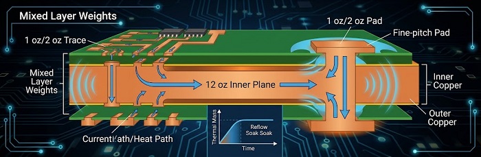
Factor in the knock-on effects too. Any board with 3 oz or more of finished copper is built on FR4 High Tg 170 only, minimum features grow as shown below, and fine-pitch parts get hard to place on heavy outer layers. Many designers put the heavy copper on inner power layers (up to 12 oz with us) and keep the outer layers lighter for component pads.
How much do trace and spacing grow with copper weight?
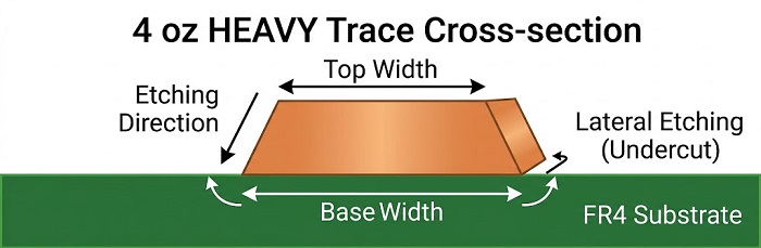
Both grow with every ounce, and above 6 oz the minimum spacing grows faster than the minimum width. The reason is etching. Thick copper stays in the etcher longer, the etchant cuts sideways as it cuts down, and the conductor ends up wider at the base than at the top. The artwork is compensated for this, and the gap has to be wide enough that the bases of two neighboring conductors never meet.
| Finished copper | Outer layer min trace / space | Inner layer min trace / space |
|---|---|---|
| 4 oz (approx. 140 µm) | 9 / 9 mil (0.23 / 0.23 mm) | 8 / 12 mil (0.20 / 0.30 mm) |
| 5 oz (approx. 175 µm) | 11 / 11 mil (0.28 / 0.28 mm) | 10 / 14 mil (0.25 / 0.36 mm) |
| 6 oz (approx. 210 µm) | 13 / 13 mil (0.33 / 0.33 mm) | 12 / 16 mil (0.30 / 0.41 mm) |
| 12 oz (approx. 420 µm) | 20 / 32 mil (0.51 / 0.81 mm) | 20 / 32 mil (0.51 / 0.81 mm) |
| 15 oz (approx. 525 µm) | 32 / 40 mil (0.81 / 1.02 mm) | Not offered (inner layers max 12 oz) |
PCBCart heavy copper minimums in mil, as published; mm and µm values are rounded conversions. For weights not listed, confirm with our engineering team.
Three things in this table catch people out.
Inner layers need more spacing than outer layers at the same weight: 12 mil versus 9 mil at 4 oz. Inner copper has to be encapsulated by prepreg during lamination, so resin must flow down into every gap between thick features. Narrow, deep channels are where resin starvation shows up, and the inner rule leaves room for the resin to get in.
These are minimums, not targets. Current-carrying traces will be far wider anyway. The minimum actually bites around component pads, in the fanout from power device pins, and between long parallel runs. On inner layers especially, a design with some margin above the minimum is easier to build than one sitting exactly on it.
The spacing rule also limits pad pitch. A quick sanity check is minimum width plus minimum space: 18 mil (about 0.46 mm) on a 4 oz outer layer, 26 mil (about 0.66 mm) on a 6 oz outer layer. If your finest-pitch part on a heavy outer layer comes close to that number, send the footprint to our engineering team before committing the layout.
Keep in mind that fab minimums are not electrical clearance. If your board runs at high voltage, the clearance and creepage required by IPC-2221 or your product safety standard may be much larger than anything in this table, and that requirement wins.
Annular ring, drill size and material choices
The minimum annular ring for heavy copper is 6 mil and the minimum drilled hole is 10 mil, but on a thick heavy copper board the board thickness usually decides your smallest practical via before either limit does.
Heavy copper boards tend to be thick ones; our range is 0.6 to 6.5 mm. A 10 mil (0.25 mm) hole near the upper end of that range is a plating challenge, because copper has to plate evenly down a deep, narrow barrel. If you plan small vias on a thick board, confirm the hole size and board thickness combination with our engineering team before you lay it out.
On annular ring, we recommend going above the 6 mil (0.15 mm) minimum on pads that carry current or anchor connectors. The ring is part of the current path between barrel and trace, and on heavy layers the same etch undercut that widens spacing also takes material off the ring edge.
For material, the rule is simple: 3 oz or more of finished copper means FR4 High Tg 170. Below 3 oz, Tg 140 and Tg 170 are both available. The High Tg requirement is not a formality. Heavy copper boards stay hot longer in every thermal cycle, and Z-axis expansion of the resin pulls on the plated barrels each time. Through-holes in thick boards with heavy inner planes are where that stress concentrates.
Heavy copper orders are built on our default layer stackup. If your design depends on a specific stackup, dielectric thickness or per-layer copper combination, raise it with our engineering team before ordering. Either way, keep copper distribution balanced: heavy copper on one side and light copper on the other gives an unbalanced board that tends to bow through lamination and reflow.
What changes on the assembly line?
The board heats unevenly. Pads tied into heavy planes are the last to reach reflow temperature, so the profile is set by those pads, and the risk moves to the small parts sitting next to them.
Thermal mass and the reflow profile
A 1 oz board with a few power parts reflows much like any other board. A board with 4 oz or more on several layers behaves differently: the planes pull heat out of the pads above them, and the whole board takes longer to come up to temperature. Run a standard profile and the small passives reflow fine while the power tab on the big plane may not wet fully.
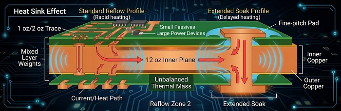
The reflow profile has to bring the slowest pad, usually the one on the heaviest copper, up to proper reflow without overheating the most temperature-sensitive part. That often means a longer soak so the heavy zone can catch up before peak, which is where the eight heating zones of our NS800II reflow oven give us room to shape the profile. The hard limit is component ratings: whatever the heavy pad needs must stay within what the most sensitive part allows. When those can't be reconciled, the fix belongs in the layout, not the oven.
Solder joints on large copper areas
Large pads on heavy planes, such as D2PAK and TO-263 tabs, power QFN exposed pads and large terminal blocks, show two typical defects: incomplete wetting where the joint never got hot enough, and voids under the thermal pad. Paste deposits are checked on our InSPIre 510B 3D SPI, which measures volume, area and height, and solder joints go through ALD515 AOI after reflow. Joints hidden under bottom-terminated power parts can't be seen optically, which is what our VIEW X2000 X-ray system is for. Inspection catches problems, though; it doesn't fix a pad that is thermally starved by design. Paste volume on large pads and the copper connection around them are worth settling at the DFM stage.
Small two-terminal parts are the other casualty. A 0402 or 0603 with one pad on a heavy plane and the other on a thin trace sees the trace side melt first, and surface tension can stand the part on end. The design fix is thermal balance: a thermal relief connection on the plane side, or matched copper on both pads. The catch is that a relief also restricts current, so on a current sense resistor you either size the spokes for the current or route both pads to equivalent copper.
Check assembly limits as well as fab limits
A heavy copper board can be within fabrication limits and still fall outside the assembly line. We fabricate boards up to 6.5 mm thick, while our G5 solder paste printer takes boards from 0.2 to 6 mm thick with a maximum area of 400 × 310 mm. If your board is thicker than 6 mm or larger than that area and also needs SMT assembly, confirm with our engineering team before you freeze the outline.
Mixed copper weights and through-hole parts
Through-hole pins soldered into heavy planes are the hardest joints on these boards to fill, because the plane draws heat away from the barrel. Pins that don't carry current should get thermal reliefs. Pins that do often need solid connections; flag them when you submit the design so they can be reviewed before the first build.
On our line, through-hole parts are soldered on a GSD-WD300T wave solder machine or a JADE MK II selective soldering system. Which one suits a heavy copper board depends on how the through-hole and SMT parts are laid out, and that is settled during DFM review, not on the first build.
Mixed weights also show up as warpage. A board with heavy copper concentrated on one side, or a heavy plane under only part of the board, can bow during reflow, which stresses joints on large parts and makes fine-pitch placement harder. The fix is in the layout: spread copper as evenly as the circuit allows and use copper balancing in lightly populated areas.
Which surface finishes are available?
For heavy copper boards we offer HASL, lead-free HASL and ENIG. Choose ENIG if the board has fine-pitch or bottom-terminated parts; the HASL options suit boards dominated by larger power parts and through-hole connectors.
| Finish | Surface flatness | Good fit | Watch for |
|---|---|---|---|
| HASL (tin-lead) | Uneven, varies with pad size | Non-RoHS products with large pads and through-hole | Not RoHS compliant |
| Lead-free HASL | Uneven, varies with pad size | RoHS products with mostly large power parts | One more high-temperature cycle on a board with high thermal mass |
| ENIG | Flat | Exposed-pad QFNs, fine-pitch parts | Higher cost, especially with large exposed copper areas |
Surface finishes available for PCBCart heavy copper boards.
OSP and immersion finishes are not on the heavy copper option list. If your current design calls for one, check whether the reason still applies once the board moves to heavy copper, or confirm with our engineering team.
Heavy copper design checklist
Run through this before you send Gerbers. Each line is something we would otherwise raise at DFM review.
| Check | What to confirm |
|---|---|
| Copper weight | Finished copper stated per layer on the fab drawing; outer layers up to 15 oz, inner layers up to 12 oz |
| Trace and space | Each layer meets the minimum for its own copper weight; inner layers use the inner values |
| Pad pitch | Finest pitch on each heavy outer layer is at least min trace plus min space for that weight |
| Electrical clearance | High-voltage spacing set by IPC-2221 or your safety standard, not by the fab minimum |
| Annular ring | 6 mil minimum; more on current-carrying and connector pads |
| Holes | 10 mil minimum drill; small holes in thick boards confirmed with our engineering team |
| Material | 3 oz or more finished copper means FR4 High Tg 170 |
| Stackup | 2 to 24 layers; thickness 0.6 to 6.5 mm; built on our default stackup unless confirmed otherwise |
| Thermal balance | Small passives with one pad on a heavy plane use reliefs or matched copper |
| Through-hole | Current-carrying pins with solid plane connections flagged when you submit the design |
| Assembly fit | For SMT assembly: board or panel 0.2 to 6 mm thick and within 400 × 310 mm, or confirmed with our engineering team |
| Surface finish | ENIG for fine-pitch or exposed-pad parts; HASL or lead-free HASL otherwise |
| Quality class | Built to IPC Class 2 as standard; any additional requirements listed at quote |
Pre-submission DFM checklist for heavy copper boards.
FAQ
Should I specify starting copper or finished copper on the drawing?
Specify finished copper, per layer. Outer layers gain copper during plating, so a foil weight on the drawing leaves the finished thickness open to interpretation, and every limit in this article refers to finished weight. If your current calculation assumed a particular thickness, state that thickness rather than just a foil name.
Is a 3 oz board treated as heavy copper?
Partly. Our heavy copper trace and space table starts at 4 oz, but the material rule starts at 3 oz: any board with 3 oz or more of finished copper is built on FR4 High Tg 170. For trace and space at 3 oz, confirm with our engineering team rather than interpolating from the table.
Can I route controlled-impedance signals on a heavy copper board?
Check with our engineering team before you commit to it. Heavy copper orders use our default stackup, and impedance on a 4 oz or heavier layer is hard to predict because the etched conductor is trapezoidal. If your design needs controlled impedance, send the requirement with your files so we can tell you up front whether the build can meet it.
What quality class are heavy copper boards built to?
IPC Class 2 is our standard for heavy copper boards. If your fab drawing calls out any other acceptance requirement, include it with your quote request so our engineering team can review it before you order.
Does heavy copper make rework harder?
Yes. The thermal mass that slows reflow also makes it hard to remove or replace a part on a large plane with a hot air tool or iron alone, because the plane keeps pulling heat away, so bottom-side preheat is normally needed. If a part is likely to be swapped during bring-up, such as a power MOSFET you may change after testing, give it some thermal isolation in the layout where the current allows.
Helpful Resources
• PCBCart SMT Assembly Equipment
• PCB Materials Available at PCBCart
• PCB Assembly Services Overview


