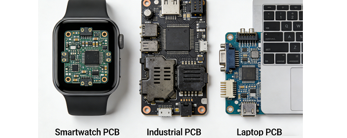
Printed Circuit Boards (PCBs) are the mainstay for powering almost all modern electronic products, ranging from the smallest digital wristwatches and wearables to industrial equipment, laptops, high-performance communication devices, and many others. The cost of creation for a PCB depends exponentially on the specifications required in the design, the materials used for the PCB, the production volume, and the complexity involved in the production process. The cost may range from as low as 50 cents for simple rigid single-layer PCBs to as high as $500 for high-end high-specialty PCBs such as rigid-flex PCBs, high-frequency RF PCBs, high-density HDI PCBs, and many others. It is very important for designers, engineers, and businesses to grasp the fundamental factors affecting the cost of PCBs, especially considering how such knowledge is vital for the production of prototypes for new products as well as for undertaking mass production processes for many different electronic products without compromising on the performance and efficiency of these products.
Key Factors That Determine PCB Costs
The price of a PCB is not a straightforward calculation, and every decision, every requirement, or every factor influences the price of a printed circuit board. The material used, number of layers, order size, and even time are just some of the many factors that need to be estimated when manufacturing a printed circuit board, as shown below:
Substrate Materials and Copper Specifications
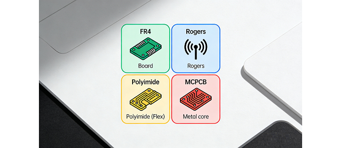
The base of a PCB is the substrate used to make the board, and the choice of substrate is one of the most expensive factors in a PCB. FR4 is the most affordable option for typical general electronics and consumer products, with all other materials costing at least 1x with FR4 as a baseline. Specialized materials for high-end PCBs, thermal PCBs, flexible PCBs, etc., will be more expensive:
· High Tg FR4 (1.2-1.5x FR4): Suitable for automotive and industrial control applications, with superior thermal properties at a moderate price increase.
· Rogers materials (3-8x FR4): RF/microwave and high-speed digital boards. Very low dielectric loss and excellent high-frequency stability.
· Polyimide flex materials (4-10x FR4): These materials form the basis of PCB flexibility and act as the core of PCBs.
· Metal core printed circuit boards (MCPCBs) (2-4x FR4): Optimized for LED lighting and power applications with industry-leading thermal performance.
Copper weight and thickness also contribute to material cost. 1 oz copper is used by industry standards and is most cost-effective. Thicker copper (2 oz, 3 oz, etc.) requires special processing and may cost 50%-200% more. It should only be used for high current power devices.
Layer Count and Manufacturing Complexity
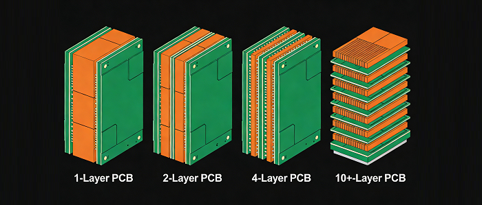
This is because the layer count has a direct effect on the actual manufacturing process. The single-layer PCBs are the cheapest and easiest to manufacture. However, the PCBs with multiple layers, such as 4, 6, 8, and 10+, become very complicated in the actual manufacturing and testing. Moreover, the cost of PCBs with multiple layers does not follow a linear pattern. For instance, when additional layers are added to the PCBs, say from 2 to 4, the cost increases by a mere 30% to 40%. However, in the case of 4-layer PCBs, their cost can be 3 to 4 times higher than the 2-layer PCBs because of complex processing and long production cycles. Moreover, the 10+ PCBs are the costliest with a cost of $3.00 to $15.00+ per square inch.
In addition to that, the other factor that influences the pricing is the complexity of the schematic design, which is not limited to the number of layers. The finer the tracing of the widths and spacing, for example, 2/2 mils instead of the standard 6/6 mils, the cost is 50-100% higher. Tight tolerances also contribute to increased cost.
Board Size and Panel Utilization
PCB size determines the commodity of raw materials required. A larger PCB for a machine requires extra money compared to a small PCB for a laptop. But a small PCB for a smartwatch, with many components and hence high functionality, costs much less to produce than a large PCB for a machine, even though the small PCB might contain many components. PCMs for a PCB can be 457 x 610mm (18 x 24”), 457 x 533mm (18 x 21”), and 533 x 610mm (21 x 24”). Panel utilization is a very important cost optimization technique in PCB production, with the PCB designed to accommodate as many PCBs as possible on a panel to reduce the cost per PCB.
Via Types And Drilling Requirements
Vias make connections between layers of a printed circuit board; their cost is heavily dependent upon the specific vias chosen, as well as their size. Through-hole vias (the standard choice that goes through all layers of the board) are the lowest-cost choice and must have a diameter of at least 0.1mm (4 mils). Specialized vias involve complex drilling and plating techniques, making them expensive:
· Blind Vias (+30–50%): Connect an outer layer to an inner layer. Minimum dimension: 0.075mm/3 mil.
· Buried vias (+50–80%): These vias are hidden in between inner layers (0.075mm/3 mil minimum.
· Microvias (+100–200%): Small vias (0.05mm/2 mil minimum diameter) for HDI boards, mobile phones.
Specialized drilling of microvias for HDI (High-Density Interconnect) boards can be 2-5 times more costly compared to a regular PCB.
Surface Finishes and Solder Mask
Surface finishes protect the PCB's copper traces and ensure reliable solderability, cost varies widely depending on the type. General-purpose baseline is HASL (Hot Air Solder Leveling, 1x cost multiplier) - excellent solderability at low cost. Lead-free HASL (1.1x) is a small premium for RoHS compliance. More advanced finishes:
· OSP (Organic Solderability Preservative, 1.2x): This is a low cost, flat finish well-suited for SMT assembly. It has a relatively short shelf life of 6 months.
· Immersion Tin (1.3x): Excellent for press-fit connectors, with a 6-month shelf life.
· Immersion Silver (1.5x): Very good for high-frequency applications, and 6–12 months of shelf life.
· ENIG (Electroless Nickel Immersion Gold, 1.8–2.5x): High-performance flat finish for fine-pitch components - e.g., BGA, wire bonding 12+ months shelf life.
Solder mask, which insulates the PCB and prevents short circuits, also has an effect on cost. Green solder mask is the most affordable option; any other color-black, white, red, blue, purple-adds 10-20% to costs, due to the special inks and production stages required. High-resolution silkscreen printing for labeling components, marking test points, or displaying warning symbols is an option, and several manufacturers offer basic silkscreen printing for free, charging a small premium for detailed silkscreen printing.
Production Volume and Economies of Scale
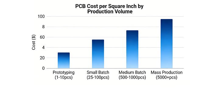
Like most products, economy of scale plays a major role in making PCBs inexpensive. Fixed manufacturing costs (such as setup costs or engineering) are divided by many units, causing the price of a single board to plummet for bulk purchases. Prototype or low-quantity orders absorb all these fixed costs, resulting in higher cost-per-square-inch pricing:
· Prototyping (1-10 pieces): $5.00 - $20.00 per square inch of material (Very high fixed cost impact).
· Small batch (25-100 pieces): $2.00 to $8.00 per square inch (reduced fixed cost effect for initial products).
· Medium batch (of 500 to 1000 pieces): $0.50–$3.00 per square inch (significant scale savings for growing production).
· Mass production (5000+ pieces): $0.20-$1.50 per square inch (lowest cost per unit, suitable consumer devices, high-volume industrial applications).
In the case of normal rigid printed boards, bulk orders can reduce the unit cost to below $1 for single-layer boards, while for multi-layer boards, a reduction of 20 to 50 percent is also achievable compared to low-volume orders.
Lead Time and Rush Production
There is an inverse proportion between PCB delivery lead time and cost. The standard production times of 3-21 days are on the lower end of the spectrum and are thus more cost-efficient for manufacturers, as they can plan more efficiently. Rush orders, whether it be for timely prototyping (1-3 days) or bulk creation, greatly increase the price, with rush orders raising their price by as much as 25-100%.
Hidden Costs and Additional Manufacturing Elements
Numerous often-overlooked factors contribute to the overall cost of a PCB, especially for custom or complicated designs:
· Engineering and setup fees:: These are one-time fees that include design rule checks (DRC) and production setup. They go from $50 to $500 for complicated boards.
· Fixture and tooling costs: Special jigs or routing templates that may be required for special designs can range from $200 to $2000. These may be useful in repeat business.
· Testing and validation: Electricity tests, such as flying probes, ICT testing, or impedance tests, guarantee the reliability of PCBs. The expenses of these tests vary between $0.50 and $5.00 per board. ICT testing, being the most advanced, is costly for low-volume orders but saves money on large orders, as it tests almost every component in under a minute.
· Electronic components and functional parts: The components used or functional parts, such as their quantity or scarcity (like resistors, capacitors, and relays), influence the pricing of a product by increasing material costs due to scarce components or necessitating a tougher design of the PCB.
· Labor costs: Skilled manpower is required for handling complex multi-layer flexible, or RF PCBs, thereby increasing manufacturing costs as opposed to using low-skilled labor to handle simple, rigid PCBs.
· Packaging: Special packaging, such as for sensitive/valuable PCBs, is also a cost driver; however, cost-effective packaging options are recommended to avoid budget overruns in the majority of cases.
· Stencils: PCB stencils, which are required for the process of SGP, are available in different formats, with better quality stencils being more expensive than ordinary ones.
Typical Cost Ranges for Different PCB Types
The cost of PCBs differs based on the types of PCBs. The most simple PCBs, also called standard rigid PCBs, are the cheapest to make. The most expensive to make are specialty PCBs and flexible PCBs. The table below illustrates the cost ranges for the most popular PCBs.
Standard Rigid PCBs
Costs for rigid PCBs increase with the number of layers and the production volume. For standard rigid printed circuit boards, the average cost of a square inch is between $0.02 and $0.05 for bulk orders. Their prices vary with the number of layers as follows:
· Single layer: $0.10–$0.50 per square inch (low volume: $1–$5 per unit; bulk: under $1 per unit).
· Double-layer: $0.20–$1.00 per square inch (low volume: $1–$10 per unit; bulk: 30–50% lower).
· 4-layer: $0.50–$2.50 per square inch (low volume: $10–$20 per unit; bulk: 20–50% lower).
· 6-layer: $1.00–$4.00 per square inch (5–7 day lead time, 3/3 mil minimum trace/spacing).
· 8-layer: $1.50–$6.00 per square inch (10–14 day lead time, 2.5/2.5 mil minimum trace/spacing).
· 10+ layer: $3.00–$15.00+ per square inch (14–21 day lead time, 2/2 mil minimum trace/spacing, for high-performance industrial/aviation electronics).
Flexible and Rigid-Flexible PCBs
Flexible PCBs are constructed with PET materials or polyimide materials, while rigid-flex PCBs are hybrid PCBs with rigid external sections and flexible internal sections. They are intended for small devices that are bendable or foldable. They are quite expensive compared to rigid PCBs due to special materials and processing:
· Flexible PCBs: Their cost is 3-10x that of standard PCBs, with the lowest cost for a single-layer flex PCB and the highest cost for a multi-layer flex PCB. The range of copper thickness for flex PCBs is 1/3oz to 3oz.
· Rigid FlexPCBs: ~7x that of standard rigid PCBs. This increased cost factor can be attributed to higher costs of no-flow prepreg material (10 times that of conventional FR4 prepreg materials); assembly complexity (PC components are kept separate and then assembled together); and lower yield rates (a combination of rigid and flex material types necessitates special expertise).
Specialty PCBs
Specialty PCBs for high-frequency RF, thick copper, HDI, and high-density have the highest price tags, being engineered for specific applications:
· High-frequency/RF PCBs: 5–15x the cost of FR4 rigid PCBs, using Rogers substrates for low dielectric loss and controlled impedance (for telecom, aerospace, and microwave equipment).
· Thick copper PCBs: 100–300% more expensive than standard 1 oz copper boards, designed for high-current power electronics (3 oz copper or higher).
· HDI PCBs: 2–5x the cost of standard rigid PCBs, relying on microvias for high-density component placement (mobile devices, advanced consumer electronics).
· Ultra-high-density PCBs: $50–$100 per square inch, for complex designs with extreme miniaturization.
· Custom flexible PCBs: Up to $500+ per square inch for highly specialized, high-complexity flexible designs (e.g., for medical implants or aerospace equipment).
Practical Strategies to Reduce PCB Cost
Fortunately, there are ways of optimizing costs associated with PCBs that don’t have to include a trade-off that affects performance or quality; many decisions, even as small as design and manufacturing decisions, can result in substantial savings. The following are steps that can be taken towards reducing PCB costs without compromising on functionality requirements.
Design Optimization
Design is the biggest area to reduce PCB costs. This is because it has the biggest opportunity:
· Minimize layer count wherever possible: Utilize smart routing and components to reduce the number of layers for a board (for instance, a 2 layer board instead of a 4 layer board).
· Adhere to normal manufacturing tolerances: Avoid ultra-fine trace widths/spacing, e.g., stick to 6/6 mil instead of going for 2/2 mil. Avoid ultra-relaxed dimensional tolerances.
· Optimize utilization of the panel: Design the PCB to conform to standard panel sizes and optimize the number of pieces per panel to arrive at a potential big money-saver.
· Apply Single-Sided Component Placement: This minimizes board assembly time since all the components are on one side, requiring only one reflow step. Additionally, this method minimizes stencil costs for a two-layer board.
Material and Finish Selection
Select cost-effective materials and finishes with the necessary performance properties for your design:
· Stick to standard FR4 substrate and 1 oz copper: This is the cheapest material combination for 90% of all electronic designs.
· Low-cost surface finish options: HASL (or 'lead-free HASL') should be chosen for general-purpose PCBs, and OSP for an SMT assembly, with the option of ENIG if fine-pitch components such as BGA are needed.
· Opt for Green Solder Mask: Skip the custom colors option since there's a 10-20% charge for non-standard solder mask inks.
· Use substitute materials: For non-critical applications, substitute CEM-3 material (a lower-cost material with similar properties to FR4) or electroless gold instead of tin-lead.
Production Planning
Leverage economies of scale and flexible lead times to reduce per-unit costs:
· Order in bulk: Combine prototype and production runs (if timelines allow) to benefit from volume discounts—even a small increase in order quantity can lower the per-unit cost significantly.
· Avoid rush production: Extend lead times to standard manufacturing timelines (3–21 days) to eliminate rush fees (25–100% of the base price).
· Consolidate orders: Combine multiple PCB designs into a single production run to spread fixed setup/tooling costs across more units.
Component and Assembly Decisions
Optimize component selection and assembly processes in order to cut both PCB and manufacturing costs:
· Use SMD instead of DIP: SMDs can be mounted, and soldered much faster (and hence cheaper) with automatic machines, reducing human labor.
· Choose components that are easy to assemble: Avoid difficult-to-assemble component types such as BGA and QFN, if possible. These parts necessitate longer inspection times and lower the yield in production, hence increasing the cost of assembling.
· Use components in reel/tray packaging: Cut tapes and loose components involve manual handling, which is a waste of expensive labor.
· Reuse known-good circuit designs: Accept minor cost increases on components (instead of designing a completely new circuit) to save on development costs for low-volume products.
· Use pre-certified modules. For wireless/RF applications, consider using only a pre-certified module-for example, Wi-Fi or Bluetooth-and avoid designing custom RF circuits. In this way, you will not have any expensive certification testing or complicated PCB design.
Avoid Hidden Costs
Work with manufacturers with transparent pricing and added services to avoid any unforeseen costs:
· Select manufacturers with complimentary DFM (Design for Manufacturability) analysis: DFM helps detect design flaws early on and thereby save on costs.
· Reuse fixtures/tooling: In the case of repeated orders, custom jigs and tools for drilling could be reused to reduce the cost of fixtures that must be built only.
· Optimize the Testing: Cost-effective tests such as flying probed test should be used for low-volume orders, while ICT tests are reserved for bulk orders.
· Negotiate the setup/engineering fees: “Many manufacturers eliminate their setup charges for bulk or repeat business, so it's always worth asking.”
Conclusion
It is a complex calculation in that it is based on hundreds of factors, including the substrate material, number of layers, order size, and delivery time. It is a balancing act between performance and manufacturability that requires avoiding over-specifying materials/designs when the end use is non-critical, using economies of scale, and sticking to standard manufacturing practices. It is also best to work with an experienced manufacturer on high-complexity boards like flex, RF, or HDI, as inexpensive manufacturing ultimately leads to poor yields and high rework costs.
When it comes to reliable and cost-effective PCB production, whether for prototyping, small-volume PCB production, or large-volume mass production, pcbcart is the trusted partner for electronic designers and businesses worldwide. As a PCB fabrication and PCB assembly service provider, pcbcart provides one-stop solutions for various PCB types, ranging from basic rigid single-layer PCBs to sophisticated high-frequency PCBs, flexible PCBs, and rigid-flex PCBs. pcbcart specializes in PCB production in accordance with the budget and performance needs of the customers and provides optimization expertise for designing as well as manufacturing high-quality PCBs at the best price. Using pcbar cart’s PCB production services, customers can efficiently and effectively translate their electronic designs into reality without incurring extra costs for PCB fabrication and assembly services.
Helpful Resources
• Components Sourcing Service
• Low-Volume PCB Assembly Service
• Altium Designer PCB Design Tutorial
• KiCAD PCB Design Tutorial
• How to Generate Gerber Files based on Different PCB Design Software
• How to Generate NC Drill Files based on Different PCB Design Software
• IC Substrate PCB


