



High-voltage sections on industrial power electronics boards — grid-scale power conversion, industrial drives, industrial IoT power modules — carry a set of design-for-manufacturability risks that don't show up on a typical mixed-signal board. This walks through five areas worth reviewing before Gerbers go to tooling: creepage and clearance, isolation component placement, solder mask/silkscreen treatment around isolation zones, test point spacing, and thermal/insulation material selection. It's a companion to PCBCart's broader industrial PCBA DFM checklist, focused specifically on high-voltage isolation design. The exact numbers for any given board — minimum creepage in millimeters, which material group a substrate falls into — depend on its working voltage, pollution degree, and material choices, so treat what follows as the questions to bring into a design review rather than a drop-in spec.
1. Creepage & Clearance Design
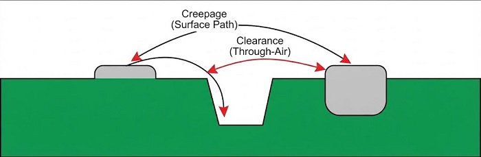
Creepage and clearance are governed by different variables and shouldn't be collapsed into one spacing rule. Clearance — the shortest through-air path — is set by the transient overvoltage category a circuit will see, not its steady-state voltage; a board can pass a DC bus check and still fail on a switching transient it wasn't sized for. Creepage — the shortest surface path — is set by the working voltage at that node, the pollution degree, and the material group (CTI) of the board and any coating in use, per IEC 60664-1. Zone transitions are a common miss: trace geometry that's fine on the low-voltage side often carries straight into a high-voltage section without being re-checked. Both should be measured as a straight-line path, not routed trace length. Where board area is tight, a slot between HV and LV zones lengthens the surface path without widening the board, per IPC-2221's slot-credit guidance, and internal layer-to-layer clearance needs the same scrutiny as the surface — a gap that looks fine visually can still be too thin between internal planes. Panel tooling and depaneling routes should also be checked against the as-depaneled board, not the panel, since rail cuts can shave real creepage off an edge that measured fine as a panel.
2. Isolation Component Placement
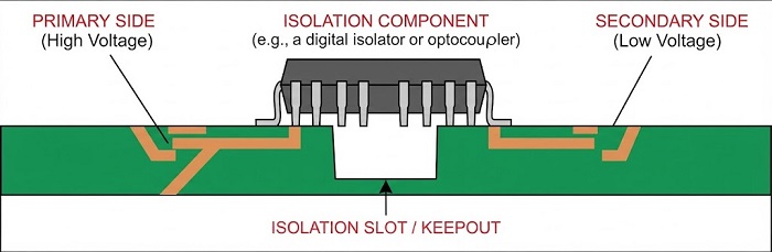
Optocouplers, isolated gate drivers, and isolation transformers only isolate as designed if the PCB boundary lines up with the component's own datasheet clearance rating — a boundary drawn off from where the part actually isolates undermines its rating regardless of what the layout shows. The same logic applies to isolated DC-DC modules: primary and secondary pin fields need a continuous keep-out slot between them, not just separated footprints, and no copper pour should cross underneath a barrier component, since a plane bridging beneath an isolator defeats it invisibly. HV connectors need enough margin that the mated contacts — not just the unmated footprint — stay clear of adjacent low-voltage circuitry. And barrier width should account for SMT placement tolerance, not just nominal position, since ordinary pick-and-place drift can erode a marginal isolation gap over a production run.
3. Solder Mask & Silkscreen Around Isolation Zones
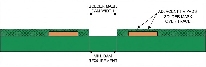
Solder mask isn't insulation for creepage/clearance purposes unless a specific coating system with its own certification is called out for that role — treating green mask as if it buys back distance is a common and risky assumption. Silkscreen deserves the same scrutiny: warning labels and reference designators printed across or beside an isolation keep-out zone can lead a reviewer to mistake the printed line for the real electrical boundary, and under humidity the ink itself can bridge a marginal gap. HV warning labels should be specified explicitly and checked for legibility after reflow, not assumed. Solder mask dam width between adjacent HV pads also needs enough margin to survive reflow thermal cycling without cracking, and should stay above the mask supplier's minimum feature size to avoid slivers — either of which can expose copper right where it matters most.
4. Test Point High-Voltage Safety Spacing
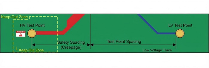
Test points don't get an exemption from creepage and clearance rules just because they sit outside the functional circuit path — an HV test point spaced like a low-voltage one is still a live high-voltage node. Beyond electrical spacing, probe access itself needs review: a test point positioned so an operator's hand ends up near a live HV node during test is a mechanical safety issue, not just a layout one. Fixture design matters too — HV and LV test points should be isolated from each other in the fixture nest, and no test point should sit inside a zone planned for potting, where post-cure access would compromise the seal. It's also worth checking that the labeled voltage on a test point matches the actual circuit, not a CAD library default.
5. Thermal Management & Insulation Materials
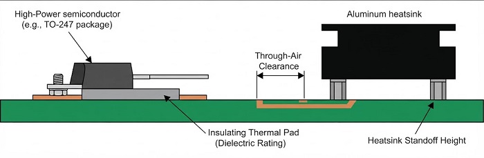
Insulating thermal pads and washers under HV components need a dielectric withstand rating that clears the applied working voltage with margin — otherwise the thermal interface material becomes the weakest link in the isolation path, not the PCB. Heatsink standoff height needs the same scrutiny, since a metal heatsink body mounted too close can close the through-air clearance to adjacent HV traces or pads. Thermal via arrays routed under an isolation barrier can create an unintended conductive bridge if they aren't checked against the barrier boundary. Where potting or encapsulation is used, it should never substitute for adequate spacing: creepage and clearance need to be verified on the bare, cleaned assembly before potting, because any shortfall gets sealed in and becomes undetectable afterward. Warpage-control fixturing during reflow is worth checking too, since a board that deflects under the fixture can shift HV connector standoffs enough that as-built clearance drifts from the as-designed value. And the insulation material's CTI rating needs to match the material group used in the creepage calculation — the calculation is only as good as that assumption.
Where These Checks Most Often Break Down
In practice, a few misses account for a disproportionate share of the rework on industrial power boards: bus bar and screw-terminal spacing sized to the connector's mechanical footprint rather than its applied working voltage once transient overvoltage is factored in; isolation keep-out zones that get visually confused with a warning label printed on top of them; and creepage/clearance sign-off that happens after potting instead of before, when any shortfall is already sealed in and unrecoverable.
Using These Categories to Evaluate an EMS Partner's High-Voltage Design Capability
Buyers can use the same five categories to gauge an EMS partner's high-voltage design capability, independent of who ultimately runs the assembly:
● Ask for a marked-up response against a real Gerber/BOM set — flagged nets and dimensioned values, not a general sign-off.
● Check whether the response distinguishes creepage from clearance, rather than applying one blanket spacing regardless of pollution degree or material group.
● Ask how isolation is verified after assembly, not just at layout — in-line methods such as 3D AOI or X-Ray for buried gaps under BGA/QFN point to a supplier reviewing manufacturability, not just a PDF.
● Confirm what happens when a violation is found — it should produce a documented finding signed off before tooling, not an informal email.
PCBCart is IATF 16949 certified for its quality management system and offers a free DFM check on submitted Gerber and BOM files as a standard pre-production step for HMLV programs.
Talk Through the Specific Numbers for Your Board
The categories above are the questions to bring into a design review — the actual minimum creepage and clearance figures for a given board depend on its working voltage, pollution degree, and the CTI of the materials chosen, and those numbers are worth working out against the specific design rather than reading off a generic table. If you'd like a second set of eyes on a high-voltage board before tooling, share your Gerber files, BOM, and the working-voltage/pollution-degree assumptions for the HV sections through PCBCart's free DFM check, and flag creepage/clearance/isolation as the priority so it's reviewed alongside the standard manufacturability check.
Helpful Resources


