



Industry: Healthcare / Life Sciences
Key Capabilities: Precision Solder Deposition · DFM Optimization · Complex Component Assembly · High-Density PCBA · Thermal Pad Engineering
Overview
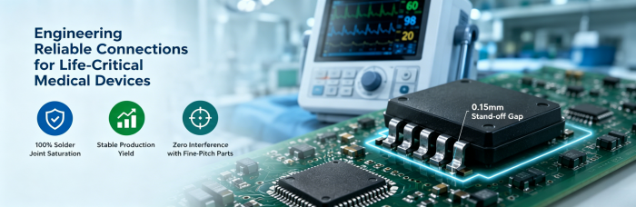
Modern medical designs often utilize components with "elevated" or "stand-off" base designs for clearance or structural reasons. In a critical medical controller project, certain ICs featured a 0.15mm stand-off height, which led to insufficient solder fill (starved joints) when using standard assembly processes. PCBCart resolved this reliability risk by re-engineering the pad aperture area—increasing it by over 100%—to ensure a full, high-strength solder joint without causing bridging on neighboring fine-pitch components.
Background
The project featured several ICs with a "raised" base design, creating a structural gap of 0.15mm between the component body and the PCB. Standard 0.12mm stencils provided insufficient paste volume to bridge this gap through capillary action. This resulted in weak mechanical connections, which are unacceptable for medical devices that must withstand vibration and thermal stress during long-term field use.
The Challenges
Mechanical Stand-off Gaps: The 0.15mm gap exceeded the standard stencil thickness, leading to "starved" solder joints.
Stencil Constraints: Increasing overall stencil thickness was impossible due to other ultra-fine pitch components on the same board that would suffer from solder bridging.
High-Density Layout: Neighboring components limited the space available for expanding the solder paste footprint.
Engineering Insight
When vertical thickness is restricted, the solution is "Horizontal Expansion." By strategically over-printing the solder paste on the pad, we provide a "reserve" of material. During reflow, the surface tension pulls this excess solder back into the pad area, effectively filling the 0.15mm vertical gap.
Optimization Strategy
Aperture Area Expansion: Increased the stencil opening area by over 100% compared to the original design to provide the necessary solder volume.
Strategic Over-printing: Implemented a controlled expansion of the solder footprint that remained within safe DFM clearances for adjacent parts.
X-ray Verification: Used X-ray imaging to confirm 100% solder saturation and robust fillet formation in the stand-off area.

Results
Full Joint Saturation: Achieved 100% solder fill, ensuring mechanical and electrical integrity.
Stable Production Yield: Successfully eliminated "starved joint" defects across all high-density production runs.
Zero Interference: The optimized solder volume was achieved without causing defects in neighboring high-density parts.
Dealing with Complex Footprints or Insufficient Solder Fill?
Leverage PCBCart’s expertise in precision solder deposition and DFM optimization to stabilize your assembly yields.


