



RF link performance on an industrial wireless gateway board is set on the SMT line, not just in the RF schematic. Assembly-stage variation eats into link budget in ways a general HMLV process plan doesn't flag by default.
A trace-adjacent pad that prints a few percent oversize, or a shield can that lands 0.1 mm off its footprint, rarely causes an outright failure the way a bridged fine-pitch QFN does. It shows up later — a few dB of unexplained insertion loss, or an intermittent RSSI drop the customer's RF engineer traces back to hardware only after ruling out firmware and antenna placement.
PCBCart's Free DFM Check flags standard manufacturability issues — pad clearance, spacing, silkscreen — before tooling. Boards with RF-specific checkpoints need review criteria on top of that: matching-network pad geometry and shield-can placement tolerance aren't things a general DFM pass is built to catch.
Where RF Link Sensitivity Meets Assembly Precision
Two assembly variables dominate the RF risk picture on a gateway board: pad geometry fidelity along controlled-impedance traces, and placement accuracy of the RF shield can relative to its ground frame. Both are dimensional problems before they are electrical ones.
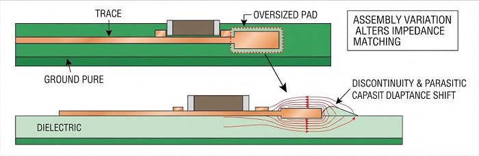
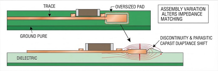
Pad size and solder mask registration on components along a matched-impedance trace decide whether that trace stays matched. A 50 Ω single-ended line (common for cellular and sub-GHz front ends) depends on a consistent relationship between trace width, dielectric height, and the copper pour it references.
A balun, matching-network capacitor, or ESD diode sitting on that line already introduces a localized discontinuity by design — assembly shouldn't add a second, unintended one. A pad printing oversize due to stencil aperture drift, or a component sitting with excess toe fillet, changes the local parasitic capacitance enough to shift the matching network's tuned frequency, particularly at the higher end of cellular bands (sub-6 GHz n77/n78).
Shield-can placement offset changes cavity volume and cross-compartment coupling in a multi-radio design. A can placed off-center relative to its ground fence alters the cavity's effective volume and the coupling between compartments — the result is inconsistent isolation between, say, a cellular PA and a co-located GNSS front end.
3D AOI can catch the offset geometrically. The electrical consequence usually only shows up during the customer's own RF validation.
Impedance Continuity Risk Points During Assembly
Reflow Thermal Stress and Micro-Displacement
Reflow-stage micro-displacement is the main way a placement offset that's well within normal SMT tolerance turns into an RF problem. Self-alignment during solder reflow is usually a benefit — it pulls a slightly misplaced 0402 back onto its pad.
But on an asymmetric or heavy component like a shield can or an RF module, differential wetting across unequal solder volumes can pull one edge more than the other, leaving a residual skew after solidification. On a digital or DC net, that skew is cosmetic. On a matched-impedance net, it isn't: the same micro-displacement changes the local return-path geometry.
The same mechanism shows up on precision analog boards elsewhere in our process documentation, where reflow-stage joint shift affects signal integrity on sensitive analog nets rather than RF ones. The takeaway carries across board types: wherever performance depends on tight geometric tolerance, the reflow profile and fixturing plan need to be qualified against that tolerance — not just against IPC-A-610 joint acceptance criteria, which weren't written with impedance in mind.
Two process controls do most of the work here: a reflow profile with controlled ramp and soak stages to reduce differential wetting forces on asymmetric components, and warpage control on the board going into reflow.
We use Synthetic Stone fixtures under boards with known warpage tendencies to hold panel flatness through the thermal cycle. A board that bows during reflow changes solder joint geometry unevenly across its surface — a harder defect to predict than a simple placement offset.
RF Shield Can Mounting: Stencil, Placement, and Post-Reflow Verification
Stencil Aperture Design for the Ground Frame
A segmented ground-fence stencil aperture, not a continuous slot, is the standard mitigation for shield-can solder joint defects. The fence itself behaves like one long, thin solder joint rather than a single pad.
Too much paste volume invites voiding and bridging between adjacent fence segments. Too little risks an open or partially wetted corner joint.
Segmenting the aperture into discrete pads with small gaps gives outgassing volatiles a path out during reflow and reduces trapped-gas voids at the corners — consistent with general ground-plane stencil-design practice, and it's where shield cans most often show marginal solder.
Placement Accuracy and Post-Reflow AOI Verification
Shield-can solder joints need two inspection checkpoints, because the can body hides them from top-down view once placed. 3D SPI verifies paste volume and print registration on the segmented fence apertures before placement.
3D AOI, run immediately after placement and before reflow, then confirms the can itself sits centered on its footprint within the placement machine's rated tolerance. Post-reflow, inspection focuses on the four corners specifically, since corner joints are both the most electrically important for shielding continuity and the most likely to show cold or open solder from the fence-segment gaps described above.
Where a corner joint can't be confirmed visually because the can body occludes it, off-line X-ray gives a non-destructive read on whether solder wetted the full fence height or bridged only partway up.
Fine-Pitch RF Module Placement and Offset Quantification
Fine-pitch RF module footprints leave less margin for placement offset than the module's package size suggests. Cellular and LoRa modules mounted as pre-certified sub-assemblies often use a castellated or LGA-style footprint with pad pitches tight enough that an offset well within general SMT tolerance can still misalign an RF or antenna-feed pad relative to its trace.
Because these modules are typically single-sourced per design and carry module-level regulatory certification, rework after reflow is more disruptive than reworking a passive. That raises the value of catching offset at inspection rather than at functional test.
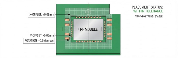
3D AOI is used here for quantified offset measurement rather than pass/fail judgment alone — reporting X/Y offset and rotation in measurable units against the module footprint, so a drift trend across a panel or lot can be caught at the placement-program level before it accumulates into failures.
MES Traceability for RF Module Lot Consistency
Lot-level traceability matters more on RF boards than on typical digital assemblies, because RF performance can vary lot-to-lot in ways that don't always fail a go/no-go functional test.
Our Smart MES system binds each RF module's lot/date code to the individual board's unique serial number at placement, with laser marking providing the physical UID on the finished board.
If a customer identifies a wireless performance inconsistency during their own RF validation or in the field, that binding lets the module lot, placement machine, and reflow run be isolated for investigation — rather than treated as a board-level unknown.
DFM Recommendations for RF-Aware Assembly
• Flag every component on a controlled-impedance trace at DFM review, not just RF-labeled parts — matching-network passives and ESD diodes are frequent blind spots.
• Segment shield-can ground-fence stencil apertures instead of a continuous slot, to manage paste volume and give volatiles an outgassing path.
• Specify four-corner AOI, and X-ray where visibility is occluded, as a standard inspection step for boards carrying an RF shield can.
• Set fine-pitch RF module placement tolerance against the module's RF/antenna pad geometry, not just its outer outline, and track 3D AOI offset data across the lot rather than board-by-board.
• Bind RF module lot/date code to board serial number at placement so any post-shipment RF inconsistency traces to a specific lot and process run.
None of this replaces the customer's own RF validation — network analyzer sweeps, radiated/conducted testing, and antenna pattern measurement stay outside assembly scope and outside our certification base.
What assembly-stage controls can do is remove the process-introduced variability that would otherwise surface as unexplained variation in that validation data.
If you're bringing a wireless gateway or multi-radio industrial IoT board into production, submit your stackup, shield-can footprint, and module placement requirements for an RF-aware assembly evaluation. We'll flag DFM risks specific to your design before first article.
Helpful Resources
• Automated X-ray Inspection (AXI) for PCB Assembly Quality
• Comparison of AOI, ICT and AXI and When to Use Them during PCB SMT Assembly


