



Pad size, pad gap and stencil aperture have to be settled together. Yield on 0201 and 01005 depends on how evenly the two pads of one part receive paste and heat, and no single dimension controls that. Start from the IPC-7351 nominal density level, keep both pads identical in copper, and size the aperture by area ratio instead of copying the pad outline. If the board cannot meet those conditions, 0402 is usually the better part to put down.
How should you size 0201 and 01005 pads?
Start from IPC-7351 at nominal density, then check the result against your own placement and print tolerances. The standard defines three density levels (Most, Nominal, Least). Most gives the largest pads and the widest process window, Least gives the smallest pads and the narrowest. We usually ask designers to begin at Nominal and drop to Least only when neighbouring parts leave no other option. A 01005 is nominally 0.4 × 0.2 mm and a 0201 is 0.6 × 0.3 mm, so a placement shift that is invisible on 0603 can be a large fraction of a pad here.
Symmetry matters more than the density level you pick. Both pads should have the same length, width and copper area, and each trace should leave its pad in line with the component axis. A 0201 with a thin trace on one pad and a pour connection on the other will tombstone however good the stencil is, because the pour side reaches liquidus later. If one terminal has to tie into a plane, use thermal relief spokes and tell us which net it is.
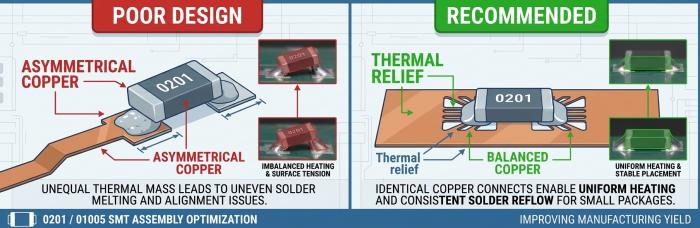
Pad definition is worth a decision too. For chip passives we normally expect non-solder-mask-defined pads, where the copper edge sets the pad size. With mask-defined pads, any registration error between mask and copper changes how much copper is exposed, and on a 0201 that can leave the two ends of one part with visibly different pad areas. That is the same imbalance as an uneven stencil, arriving through the fabrication side. If your fabricator's mask registration is loose, say so early, because it changes what pad and gap you can safely draw.
Three habits we check in DFM before anything is released to the line:
No open via inside a 0201 or 01005 pad. Solder wicks down the barrel and the paste volume on that pad drops.
A solder mask dam between the two pads only if your fabricator can hold mask registration well enough to keep it. A dam that lands on the pad edge is worse than none.
A footprint from a verified library, not a scaled-down 0402. Scaling rarely preserves the gap between the pads, which is the dimension that most affects mid-chip solder balls.
We don't publish a universal pad table. The right lengths and gaps depend on the termination dimensions in your component vendor's drawing and on your mask registration, so confirm with our engineering team before you freeze the library part.
How does spacing affect tombstoning and bridging?
Tombstoning starts when the pad that melts first pulls one end of the part upright, and three things decide which pad that is: paste volume, copper mass and where the part sits relative to the pads when reflow begins. Bridging is the opposite problem, too much paste or too little clearance between neighbouring pads or neighbouring parts.
On spacing, the IPC courtyard is a minimum, not a target. Around 01005 clusters we prefer more room than the courtyard when the board allows it, for two practical reasons. A tall neighbour shades the fillet from the AOI camera angle, and it also crowds the placement nozzle. If a 01005 sits against a connector shell or an inductor, the joint may be fine and still be impossible to verify.
Orientation is the cheap lever people forget. A 0201 beside a large thermal mass, such as a shield frame, a heavy connector or a big ground pad, sees uneven heating across its two pads if one pad faces the mass and the other does not. Rotating the part 90 degrees so both pads see the mass equally often removes the problem without touching the stencil. When the layout allows it, also keep the parts of one cluster in the same orientation so the print behaves the same way on every pair.
| Symptom after reflow | First thing we check | Usual fix |
|---|---|---|
| One end lifted (tombstone) | Paste volume difference between the two apertures, then copper connected to each pad | Identical apertures, thermal relief on the heavy side, trace entry in line with the part |
| Part skewed or rotated | Placement offset, then pad gap | Local fiducials, check gap against the part's termination drawing |
| Bridge between neighbouring parts | Pad-to-pad spacing and aperture overhang past the pad edge | Pull the aperture back from the pad edge, add spacing |
| Solder balls beside the body | Gap between pads and paste volume under the body | Reduce the aperture on the inside edge, review the gap |
| Open or starved joint | Area ratio and SPI volume | Thinner foil or a larger aperture, covered below |
We covered the general causes of these defects in our common SMT defects article, so this piece stays with what changes at 0201 and 01005.
How thin should the stencil be, and what area ratio do you need?
Choose the foil thickness from the area ratio of the smallest aperture on the board, then check that your largest packages still get enough paste. Area ratio is the aperture opening area divided by the area of its walls. For a rectangular opening of length L and width W in foil of thickness T, that is (L × W) / (2 × (L + W) × T). For a square opening of side W it reduces to W / (4T). A common minimum is 0.66, and below it paste release becomes inconsistent.
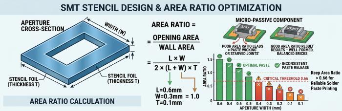
The squeeze at 01005 comes straight out of that formula. Shrinking an aperture to cut paste volume also lowers its area ratio, so aperture reduction cannot be used freely on small pads. Only a thinner foil raises the ratio again, and a thinner foil prints less paste on every other pad of the board. Halve the thickness and the ratio doubles for any given opening. Meanwhile, the QFN thermal pad or the connector two inches away wants the opposite.
There are a few ways out, and none is free. One thin foil for the whole board works when the biggest paste demand on the board can live with it, and the first-article SPI data tells you quickly whether it does. A stepped foil, thinner in the micro-passive zone, is a common technique, though you should confirm with our engineering team whether it suits your panel. We also run a MYCRONIC jet printer, which does not depend on a stencil aperture; whether it is the right fit for a given board is an engineering call that we make after seeing the files. The fourth option is the unglamorous one, moving the non-critical passives back to 0402 so the stencil only has to solve one problem.
Aperture shape gets more attention than it deserves. Reduced and shaped openings are common on 0201, but what protects yield is that the two apertures of one part are identical and registered to their pads. A well-shaped aperture printed off-centre loses to a plain one printed in position. Wall quality matters too, since rough laser-cut walls hold paste back at these sizes. Foil thickness, paste powder type and any coating are all board-specific, so confirm them with our engineering team instead of copying a number from a datasheet.
Print process settings sit on top of all this and are easy to blame on the design. Stencil underside cleaning is a good example. Residue around a small opening smears onto the next board and shows up as a bridge or a volume swing, and no pad change fixes it. SPI trend data across consecutive boards tells you whether the cleaning interval is the problem, which is why we read it before suggesting a layout change.
What should placement and 3D SPI/AOI catch on micro passives?
Check paste first, then placement, then the reflowed joint, and treat the first two as the ones that decide yield. With 3D SPI we look at paste volume, height, area and offset per pad. On 0201 and 01005, the number that matters is the difference between the two pads of one part. Two pads that each pass their own limits can still be unbalanced as a pair, and an unbalanced pair is what tombstones.
Placement is the next place the margin disappears. Feeders and nozzles for 01005 are a different class of setup from 0402, which is one reason to run a first article before the full lot and read the SPI data for the micro-passive area, not only the AOI result. Local fiducials near a dense cluster help the machine correct for local board distortion that the global fiducials cannot see.
After reflow, AOI catches missing parts, shifted or rotated parts, tombstones and bridges. Chip-passive joints are visible from above, so AOI covers them, and offline X-ray adds little for these parts. The reflow profile on our JTR-1200D-N is set per board, and a profile that heats too fast can tombstone a perfectly symmetric design. If tombstones cluster in one corner of the board, look at the print in that corner before you touch the profile, because SPI will usually show the volume mismatch there.
One habit saves a lot of argument later. When SPI and AOI disagree, for example paste looked balanced but a part still lifted, compare the two data sets for that exact reference designator before changing anything. The cause is usually one of the three we listed earlier, copper mass, placement offset or heating, and the data tells you which one in a few minutes. Changing the stencil and the profile at the same time makes the result impossible to read.
When should you stay with 0402?
Stay with 0402 when the board gains little from the space saved and loses margin from the smaller part. We usually ask one question first: which nets actually force the 0201? If the answer is bypass capacitors under a fine-pitch BGA, use 0201 there and keep 0402 elsewhere. If the answer is that the whole BOM was shrunk to save a few square millimetres, go back.
td {white-space:nowrap;border:0.5pt solid #dee0e3;font-size:10pt;font-style:normal;font-weight:normal;vertical-align:middle;word-break:normal;word-wrap:normal;}
| Condition on your board | Stay with 0402 | Move to 0201 or 01005 |
|---|---|---|
| Layout room | Routing and courtyards fit with space to spare | Spacing is what blocks the layout, for example around BGA escape routing |
| Pad symmetry | One pad is forced onto a plane or a trace entry cannot be balanced | Copper on both pads can be made identical, with thermal relief where needed |
| Paste demand | The same stencil must print large packages that need thicker foil | Micro passives dominate, or a stepped foil or jet printing is workable |
| Part availability | The value or voltage rating is not offered in the smaller size, or DC-bias derating has not been checked | The part exists and its derated value still meets the circuit |
| Rework | You expect hand rework on the passives | Rework is controlled and rare |
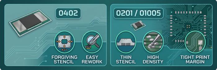
A practical order of decisions helps on a first spin. Fix the pad symmetry and the orientation in layout, then decide the foil thickness from the smallest aperture, and only then ask whether the biggest package on the board can live with that foil. If it cannot, the cheapest change is usually to give some passives a larger size. On a prototype lot we would rather see a few 0402 parts than a board where tombstones hide the real problem, and you can shrink on the next revision once the SPI and AOI data show how much margin the micro-passive area has. Hand rework on 0201 and 01005 is also a poor bet, since a single touch can displace the neighbours, so a design that expects rework should lean toward the larger size.
Capability is the other limit. The SMT Packages page lists 0201 and 01005 among the chip sizes we assemble. Anything smaller than 01005 is not on that page, so ask us before you commit a design to a package below it.
FAQ
Do 0201 and 01005 need a different solder paste?
Often, yes. Finer powder generally releases better from small apertures, but the right type depends on your smallest opening and your alloy. Confirm the paste choice with our engineering team once we have your paste layer.
Can I put a via next to a 0201 pad?
Next to it, yes, with enough room that the via and the pad cannot share solder. Inside the pad, avoid it unless the via is filled and capped. If you cannot move it, send us the layout and we will tell you what we see.
What should I send so you can review my micro-passive pads before quoting?
Gerber files including the paste layers, a BOM with exact manufacturer part numbers, the pick-and-place file, and an assembly drawing that marks which parts are 0201 or 01005. The exact part number matters because pad geometry depends on the termination drawing.
Will you change my footprints?
Not without your sign-off. Our DFM review flags pad, gap and symmetry problems and you decide what to change. We do not offer schematic design.
How many local fiducials does a dense cluster need?
It depends on cluster size and panel layout. Confirm the number and placement with our engineering team during DFM review.
Helpful Resources
Design Requirement of SMT PCBs Part One: Bonding Pad Design of Some Ordinary Components
Understanding PCB Stencil Thickness and Its Impact on Solder Volume
The Impact of 01005 Component Placement on SMT Line Accuracy


