



for ATE load boards, probe interface boards, DIBs, and burn-in boards, the right EMS partner is judged less on headline capability lists and more on four specifics — coplanarity control after reflow, oblique-angle X-ray inspection capability, MES traceability granularity down to the individual board/UID level, and engineering turnaround on revision changes. Consumer-electronics-scale EMS providers can usually check the equipment box; far fewer can execute all four consistently on 5–200-piece lots with weekly ECO churn.
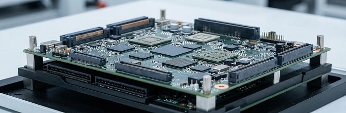
Why Does Sourcing PCBA for Semiconductor Test Equipment Break the Standard EMS Model?
Test equipment OEMs — building probe cards, load boards, handler interface boards, and burn-in racks — run a sourcing profile that doesn't match the volume-driven assumptions most EMS providers are built around.
Lot sizes are small and recurring, not one-time. A single program might need 10–50 boards per revision, repeated across multiple stepping/tester-platform variants.
Mechanical precision matters as much as electrical function. Warpage, coplanarity, and fine-pitch BGA/QFN placement accuracy directly affect probe/socket contact reliability — a defect mode most consumer EMS lines aren't set up to catch.
Revisions are frequent. Pinout changes, socket updates, and DIB stack-up tweaks happen far more often than in a mature consumer product, making engineering response time a recurring cost rather than a one-time qualification hurdle.
This combination — small lots, tight tolerances, frequent revisions — is the definition of high-mix, low-volume (HMLV) work, and it rewards a different supplier profile than a high-volume SMT line.
What Should Buyers Actually Evaluate Before Issuing an RFQ?
How well does the supplier control coplanarity and warpage?
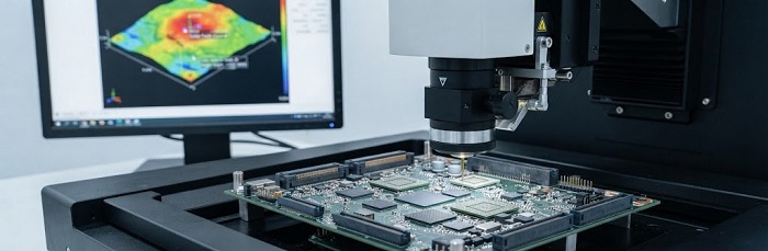
Load boards and DIBs are often large-format, multilayer, and populated with fine-pitch BGAs adjacent to connectors and stiffeners — a layout that concentrates thermal stress unevenly across the panel. Ask specifically:
What fixturing constrains warpage during reflow on large or asymmetric boards? (Synthetic stone fixtures are one approach — ask what a given supplier actually uses, not just whether they claim to "control warpage.")
Is post-reflow coplanarity measured and recorded per board, or only sampled?
Does 3D SPI feed back into paste-deposition adjustments in a closed loop, or is it just a pass/fail gate?
Can the supplier actually do oblique-angle X-ray, or just top-down?

Voiding under BGAs and QFNs — and, on load boards, solder integrity under socket/connector shadowing — is often invisible to a standard top-down X-ray view. Oblique-angle (multi-angle) inspection lets an inspector see under a component from a shifted viewpoint rather than straight through it. This matters on ATE boards specifically because connectors and sockets frequently sit close to BGA packages, creating shadowing top-down X-ray can't resolve, and because voiding thresholds on high-frequency signal paths are often tighter than general industrial tolerance.
The more useful question isn't "is oblique-angle standard or an add-on" — reasonable suppliers may price it separately without being illegitimate. It's whether the supplier can explain, for your specific board, why a given component layout does or doesn't need it. A supplier who applies oblique-angle inspection based on shadowing risk from your actual stack-up and component placement is doing real process control; one who can't articulate that risk assessment either way is applying inspection reflexively rather than to the defect mode it's meant to catch.
How granular is the MES traceability, and does it track use, not just build?
Standard MES traceability records what went into a board at build time — component lots, operator, station, timestamp. ATE and burn-in boards benefit from a further layer: tracking probe-cycle counts and rework history against a specific board UID over its service life, since load boards get reworked and redeployed rather than scrapped after one use. Ask whether traceability ties to a physical UID (laser-marked or otherwise) that survives rework, whether records can be pulled per-board on demand rather than only per-lot, and whether the MES logs rework history or just the original build record.
How fast — and how structured — is engineering response to a revision?

Frequent ECOs mean the real cost driver isn't the first article; it's every subsequent revision. A useful proxy question: how is a stack-up or pinout change handled — through a re-quote and documented DFM re-check, or informally? Suppliers built around long, stable production runs often lack a repeatable process for this, simply because they rarely need one.
How Do You Spot a Supplier That "Says Semiconductor" but Runs a Consumer Line?
A few practical tells separate genuine ATE/semiconductor-test experience from a consumer-electronics EMS line with the word "semiconductor" added to a capabilities page:
Vague on inspection specifics. A supplier that lists "AOI, X-ray" without describing oblique-angle capability, voiding thresholds, or SPI closed-loop behavior in mechanism-level terms is likely describing consumer-line QC, not test-board-grade QC.
No differentiated warpage/coplanarity answer. If "how do you control warpage on a large multilayer board" gets the same generic answer regardless of board size, layer count, or component asymmetry, the supplier likely hasn't internalized why probe/socket contact reliability depends on it — they're describing general SMT process control, not something built around test-board tolerance requirements.
No comfort with small, recurring lots. If MOQ conversations default toward volume discounts and steady forecasts, the cost model isn't built for 10–50-piece recurring lots.
Traceability stops at the lot, not the board. Per-lot-only traceability is standard for consumer SMT; per-UID, rework-aware traceability signals test-equipment-specific process maturity.
What Order Profile Fits an HMLV Specialist vs. a High-Volume Line?
As a general framework rather than a fixed rule, HMLV-focused EMS capacity tends to fit best where lot sizes run from single-digit prototype quantities up to a few hundred pieces per revision (rather than steady five- or six-figure runs), board complexity includes fine-pitch BGA/QFN and tight mechanical tolerances, revisions occur quarterly or more often, and traceability needs to extend to individual board history over a service life rather than just a build record.
A high-volume EMS line, by contrast, is usually the better economic fit once a design stabilizes and quantities scale into steady high-volume monthly production — a transition point worth planning for explicitly rather than assuming either supplier type covers the whole product lifecycle.
Supplier Evaluation Checklist
1. Before sending an RFQ, it's worth getting direct answers — in writing, not just verbally — on:
2. What specific warpage/coplanarity control method is used on large or asymmetric board formats?
3. Can the supplier explain, for your specific stack-up and component placement, whether oblique-angle X-ray is needed and what voiding threshold triggers a reject?
4. Is 3D SPI data closed-loop into paste deposition, or sampled/informational only?
5. Does MES traceability track per-board UID history, including rework, or only per-lot build data?
6. What is the documented process for handling a mid-program ECO — re-quote, DFM re-check, timeline?
7. What lot-size range does the supplier consider "normal" versus "exception pricing"?
8. Which certifications does the supplier actually hold, and which quality frameworks (e.g., IATF 16949) do they reference — confirmed directly, not inferred from a capabilities page?
Helpful Resources
· ESD Control & Handling Protocols for Semiconductor Test Board Assembly
· MES-Driven Lifecycle Tracking for ATE Interface Boards: Probe-Cycle and Rework History
· AXI Test (X-Ray Inspection Capability)


