



Semiconductor test boards — load boards, probe cards, and burn-in/ATE interface boards — carry component classes that are disproportionately vulnerable to electrostatic discharge. Precision resistor networks used for calibration accuracy, high-speed signal conditioning ICs, and low-noise analog front-end devices often sit at ESD sensitivity thresholds well below the general assumptions applied to standard industrial PCBA. A single uncontrolled discharge event during handling, placement, or post-reflow inspection can degrade a device's parametric performance without producing a hard failure — a latent defect that only surfaces after the board is deployed in a test cell, where it is far more expensive to diagnose than at the assembly stage.
For an HMLV (high-mix, low-volume) EMS provider building ATE and semiconductor test interface boards, ESD control is not a single inspection gate but a chain of custody that has to hold from incoming material receipt through final packaging. Below is how that chain is structured, and where the control points sit.
Why Test Board Components Carry Elevated ESD Risk
Two component characteristics on semiconductor test boards raise ESD exposure relative to typical industrial assemblies:
Precision resistor networks. Thin-film and matched resistor arrays used for calibration and reference accuracy are sensitive to charge-induced drift. Unlike catastrophic ESD failure, drift-type damage can leave a resistor network functional but out of tolerance, which is difficult to catch without a full parametric re-test.
High-speed signal and low-noise devices. Components handling high-speed digital or precision analog signal paths — comparators, precision op-amps, and signal-conditioning ICs — frequently carry HBM (Human Body Model) sensitivity classifications at the lower end of JEDEC JS-001 categories, meaning routine handling without controls presents real risk.

Because these failure modes are latent rather than immediately observable, ESD control on test board programs has to be treated as a preventive discipline rather than something correctable through post-assembly testing alone.
Workstation and Process Control Measures
ESD-sensitive test board builds are run under a layered set of physical and procedural controls at the assembly workstation level:
Grounding and Personnel Controls
Continuous-monitoring wrist straps at manual placement, rework, and inspection stations, with grounding verified at shift start.
ESD flooring and dissipative worksurfaces tied to a common ground reference, avoiding isolated ground points that can create potential differences between adjacent stations.
ESD-safe garments (heel grounders or smocks) for operators handling boards outside of strap-monitored fixed stations, such as during transfer between process steps.
Equipment-Level Controls
Ground reference verification at the MYCRONIC jet printer/dispenser station and at manual and semi-automated placement points where components are directly handled.
Ionization at stages where non-conductive packaging materials or trays are present, since static charge on insulative surfaces cannot be drained through grounding alone.
Controlled handling protocols during 3D SPI and 3D AOI inspection stages, where boards are frequently repositioned for camera angle or manual verification — a point where inconsistent handling discipline commonly introduces risk if not procedurally enforced.
Packaging and Transport
ESD-shielding bags (typically metal-out or moisture-barrier ESD bags for moisture-sensitive devices) for board-level and component-level transport between process stages and prior to outbound shipment.
Conductive or dissipative totes for intra-facility movement, replacing non-rated general-purpose containers.
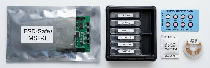
Desiccant and humidity indicator cards where components carrying both ESD and moisture sensitivity classifications are present, since packaging integrity affects both risk categories simultaneously.
Incoming Material Control: Isolating ESD-Sensitive Lots at IQC
ESD control on the finished board is only as reliable as the handling discipline applied to incoming components. At IQC (incoming quality control), ESD-sensitive material is separated from general stock through:
Segregated storage locations for components carrying ESD-sensitive markings, kept in original manufacturer ESD packaging until kitting, rather than being repackaged into general-purpose bins.
Lot-level identification at receipt, tagging ESD-sensitive lots so downstream kitting and placement operations trigger the correct handling protocol automatically rather than relying on operator judgment at each transfer.
Restricted access to open-bag stock, since once an ESD-sensitive component's original packaging is opened, exposure risk begins accumulating with each subsequent handling event — limiting the number of times a lot is opened and re-sealed reduces cumulative risk.
This segregation matters most on HMLV programs, where a single facility may be running ESD-sensitive semiconductor test board lots alongside general industrial PCBA in the same shift — the isolation step prevents cross-contamination of handling discipline between programs with different risk profiles.
MES Traceability for ESD-Sensitive Material Handling
Handling history for ESD-sensitive material is recorded through the Smart MES platform, using UID-level traceability and laser marking to tie each board or panel to its process history rather than relying on batch-level paper travelers alone. For ESD-sensitive builds, this traceability layer typically captures:
Which workstation and operator handled the board at each process step, correlated against wrist-strap and grounding verification logs where integrated.
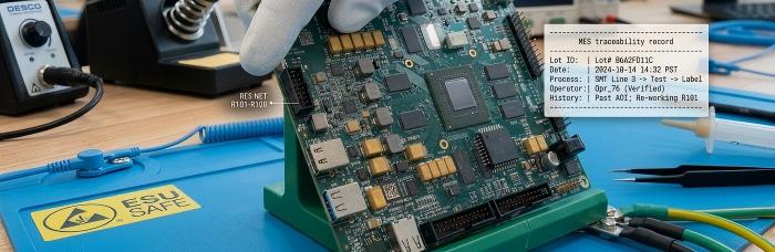
Time-stamped movement between ESD-controlled zones, supporting root-cause investigation if a parametric failure is later traced back to a specific handling window.
Component lot association at the UID level, so that if an incoming lot is later flagged (for example, following a supplier notification), affected boards can be identified without a full-batch recall.
This level of traceability is particularly relevant for semiconductor test board customers, since a board with a latent ESD-induced parametric drift may not fail until it's already been integrated into a test cell — at which point UID-level history is what allows the failure to be traced back to a process step rather than treated as an unexplained field return.
Planning a Sensitive-Device Test Board Program
Semiconductor test boards carrying precision resistor networks, high-speed signal devices, or other HBM-sensitive components benefit from ESD control protocols scoped to the specific device classifications on the BOM rather than applied as a generic checklist. If you're planning an ATE or semiconductor test interface board build with ESD-sensitive components, submit your project details for a manufacturing assessment, and our engineering team will review handling and traceability requirements specific to your component set before quoting.
Helpful Resources
• X-Ray Oblique-Angle Inspection Protocols for Multi-Layer ATE Interface Board BGA
• Why Calibration and Test Matter for Sensor and MEMS Modules
• ESD Control Protocols in PCBA Assembly for Sensitive Medical Sensor Boards
• Commonly-Used Measures to Control ESD Damage in SMT Assembly Workshop


