



Semiconductor ATE and burn-in boards operate under tolerances most industrial PCBA never encounters: probe contact windows measured in microns, thermal cycling into the hundreds of degrees, and zero margin for intermittent failure once a board is loaded into a test cell. A design review that passes for a general industrial control board can still produce a non-functional ATE interface board. The checklist below organizes pre-production DFM review into five verification categories, each targeting failure modes specific to test and burn-in hardware.
Coplanarity and Warpage Verification
Coplanarity and warpage sit at the top of ATE-specific risk because both translate directly into probe contact failure and component placement shift — the two most common root causes of test-board field returns.
Confirm maximum allowable board bow and twist per IPC-A-610 Class 3 criteria before panelization is finalized.
Specify coplanarity tolerance for BGA and QFN sites relative to the socket or probe card interface, not just relative to the board plane.
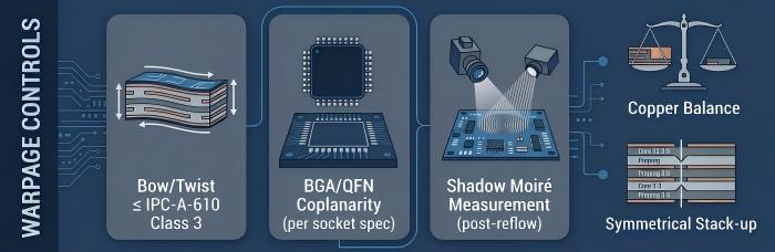
Flag high-density fine-pitch BGA regions for reflow profile validation using synthetic stone fixtures rather than standard metal jigs, since fixture-induced warpage during reflow is a common source of post-solder coplanarity drift.
Require post-reflow warpage measurement data (via shadow moiré or equivalent) as an exit criterion before a design is released to volume.
Review panel layout for asymmetric copper distribution that can bias warpage direction across the panel.
Verify solder mask and copper balance on opposing layers near large BGA fields to reduce differential shrinkage.
Identify any large open copper pours near probe interface zones that could locally stiffen or relax the board and skew local flatness.
Confirm stack-up symmetry has been checked specifically in the probe/socket keep-in zone, not only at panel center.
Why this matters for ATE specifically: a probe card or pogo-pin interface has a fixed vertical travel window. Even sub-100-micron coplanarity deviation at a BGA or fine-pitch QFN can push individual balls or leads outside that window, producing intermittent opens that only surface under thermal load — the failure mode burn-in is meant to catch, not cause. Warpage introduced during reflow compounds this: it shifts component-to-pad registration during solder solidification, which 3D SPI and 3D AOI closed-loop inspection can flag post-print and post-placement, but only when the inspection tolerance is set to what the test interface actually requires, not a generic default.
ESD and Static Discharge Protection
ATE and burn-in boards frequently carry unpackaged or bare-die interfaces and low-threshold analog front ends, raising ESD sensitivity well above typical industrial assemblies.
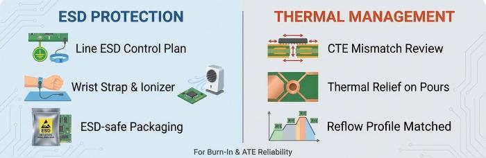
Confirm the ESD control plan covers the assembly line, not only the design file — grounding, ionization, and wrist-strap verification at each handling step.
Review component ESD sensitivity classification (per JEDEC/JESD22-A114 where applicable) against the line's handling procedures.
Verify test and calibration connectors intended for field or lab use have ESD protection placed as close to the connector as layout allows.
Confirm static-dissipative or conductive packaging is specified for board transport between assembly, inspection, and shipping.
Flag any exposed probe pads, gold fingers, or calibration test points lacking ESD protection in the schematic.
Require ESD audit sign-off as a discrete checklist item prior to first-article build, separate from general process audit.
Thermal Management and CTE Considerations
Burn-in boards see repeated thermal cycling from ambient to elevated test chamber temperatures, which makes coefficient of thermal expansion (CTE) mismatch a primary long-term reliability risk rather than a secondary concern.
Confirm solder alloy selection accounts for the burn-in chamber's rated temperature profile — standard SAC alloys should be reviewed against the actual dwell time and cycle count, since fatigue behavior differs from single-reflow assumptions.
Review CTE mismatch between socket/connector housings and the PCB substrate at high pin-count interface zones.
Verify thermal relief and copper pour design near high-power test-load components to avoid localized hot spots during extended cycles.
Confirm reflow profile parameters on the reflow oven are matched to the specific alloy and component thermal mass, not a generic profile carried over from a prior job.
Flag large connectors or heat-sink hardware for mechanical stress review at their solder joints under repeated thermal cycling.
Review via-in-pad and thermal via placement under high-power components for consistency with the dissipation requirement.
Confirm rigid-flex transition zones used in burn-in fixtures exclude components and copper features from the bend radius — placement inside the flex bend zone is a recurring root cause of early-cycle fatigue failure.
Require documented thermal cycling criteria (cycle count, temperature extremes, dwell time) be shared with the assembly partner before first-article build, so process parameters align to the actual use profile.
Test Point and Probe Interface Design
The probe or socket interface is the single point where mechanical, electrical, and process tolerances converge, making this section the most failure-dense part of the checklist.
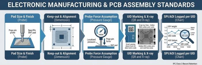
Confirm test point pad size and plating finish match the probe or pogo-pin manufacturer's specification, not a generic ENIG default.
Verify test point placement maintains adequate keep-out from adjacent components to prevent probe overtravel damage.
Review pad-to-pad spacing at high-density probe fields against the probe card's physical pitch limits, including manufacturing tolerance stack-up.
Confirm flying-probe or ICT accessibility has been reviewed for every net requiring in-circuit test, not only the nets flagged by the schematic.
Flag any test points located under or immediately adjacent to tall components that could obstruct probe access.
Verify socket alignment features (guide pins, keying) are specified with tolerances consistent with the board's warpage and coplanarity limits from Section 1.
Confirm surface finish selection accounts for repeated probe contact cycles, since finish wear under multiple insertion cycles differs from single-touch field connector wear.
Require a documented probe-force and insertion-cycle assumption be part of the design record, so the assembly partner can flag any mismatch with actual test cell equipment before build.
Traceability and Documentation
Confirm UID marking location and laser-marking parameters are defined in the design package for MES-based traceability.
Verify traceability data captures component lot and date-code information for ESD, thermal, or field-return investigations.
Require X-ray inspection data (BGA/QFN voiding, including oblique-angle imaging where hidden-joint geometry requires it) be retained in the build record for high-risk assemblies.
Confirm 3D SPI and 3D AOI inspection results are logged against board UID rather than batch-level summary only.
Review documentation package for completeness against IPC Class 3 record-keeping expectations.
Confirm design revision control ties to the traceability record, so mid-run engineering changes are captured against the UID range affected.
From Checklist to Supplier DFM Capability Assessment
A checklist like this one has a second use beyond pre-production review: it works as a structured way to evaluate whether a prospective assembly partner actually has the process capability the design requires. Rather than asking a supplier generically whether they "support ATE work," a design team can walk each section — coplanarity measurement method, ESD line controls, thermal profile documentation, probe interface tooling, UID-level traceability — and ask the supplier to demonstrate capability item by item. A partner who can speak specifically to fixture selection for warpage-sensitive reflow, closed-loop SPI/AOI tolerance configuration, and oblique-angle X-ray availability for hidden BGA joints is signaling genuine HMLV test-equipment experience, not general SMT capacity relabeled for a specialized market.
Teams running this assessment against their current or prospective supplier are welcome to request a capability walkthrough from PCBCart's engineering team against any of the five categories above.
Delivery Format and Next Step
This checklist is intended for use as a static, printable pre-production audit form — a document engineering and quality teams can walk through line by line before a design is released to build, and attach to the design record for traceability. It is not a live dashboard or a subscription report.
Design teams evaluating a new ATE or burn-in board are welcome to submit Gerber files to PCBCart for a DFM pre-review and quote, where the coplanarity, thermal, and probe-interface risk areas above are assessed against the specific design before committing to build. Reach out to PCBCart's engineering team to start a DFM pre-review, or request a quote directly for an upcoming ATE or burn-in PCBA build.
Helpful Resources
• High-Mix Assembly for Semiconductor ATE: CoC Socket Boards & Fine-Pitch BGA Coplanarity
• First Article Inspection Service on All PCB Assembly Orders
• How Risky Is Placing a First Order With an Unfamiliar Assembler?
• Free PCB DFM Check and Checklist for PCB Assembly


