



Industrial wireless devices such as gateways, sensor nodes and remote I/O modules put radios, switching regulators and high-speed digital circuits in a small enclosure. EMC performance is mostly decided at the layout and enclosure stage. But a design that looks sound on paper can still fail pre-compliance measurements because of small assembly variations that nobody saw on the line.
This article covers the EMC risk factors that the assembly process can introduce or prevent, and the inspection and first-article practices that catch them early. It does not cover EMC certification testing, which is performed by the OEM or a qualified third-party laboratory.
What Assembly Can and Cannot Control
Assembly cannot fix a poor return-path design, a marginal filter topology or an inadequate enclosure seam. It can, however, make sure that the board matches the design intent: every grounding connection made, every shield seated, every decoupling and filtering component present, correctly placed and correctly soldered.
A board that departs from its design intent in one of these ways may pass functional test and still radiate or couple noise differently from the engineering sample. Pre-compliance results then become hard to interpret, because the engineer cannot tell whether a failure is a design problem or a build problem.
Assembly-Introduced EMC Risk Factors
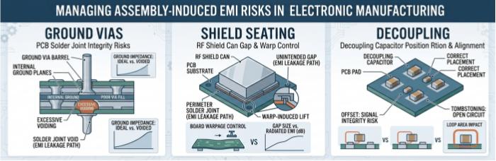
Ground Via and Ground Pin Solder Integrity
Low-impedance return paths depend on ground connections being complete. In assembly, the relevant failure points include:
Through-hole connector shells, shield tabs and ground pins with insufficient hole fill
Exposed ground pads on QFN and similar packages with excessive or poorly distributed voiding
Ground-connected pads where paste deposition was marginal
A joint that is electrically continuous but mechanically or thermally weak can increase ground impedance, and this is hard to see in a visual check. For through-hole grounding features, automated selective wave soldering with nitrogen protection supports repeatable hole fill. For hidden joints, off-line X-ray with oblique-angle capability allows void and fill assessment under QFN and BGA packages.
Shield Can Seating and Gap Control
RF shield cans work only if they sit flat and make continuous contact around their perimeter. Assembly-stage gap sources include:
Placement offset or rotation
Component tilt during reflow
Board warpage that lifts a corner of the frame
Rework that disturbs a previously placed shield
An unintended gap acts as a slot that can leak energy at frequencies related to its length. Warpage control during reflow is therefore part of EMC risk management, not only a coplanarity matter. Synthetic stone fixtures help keep thin or asymmetric boards flat through thermal processing, and a multi-zone reflow oven such as the JTR-1200D-N lets the profile be tuned for mixed thermal mass, so large shield frames and small passives reach reflow together.
Shield joints, especially at corners, deserve explicit inspection criteria rather than a general “placement OK” judgment.
Decoupling and Filter Component Omission and Offset
Decoupling capacitors, ferrite beads and RF filter elements are small and numerous, and they are among the components most likely to be skipped by a feeder error or displaced by a paste or placement issue. A missing 0402 or 0201 capacitor rarely causes a functional failure. It can, however, raise supply-rail noise or weaken a filter without any obvious symptom, so the defect passes through to EMC measurement as a “design problem.”
Position matters too. A decoupling capacitor shifted away from its pad loses part of the loop-area benefit the layout was designed to provide. Offset and tombstoning on these parts should be treated as functional defects, not cosmetic ones.
Where 3D AOI Fits: Verifying Presence and Position
The risk of an omitted component is that it is invisible downstream. Once the board is through reflow, nothing in a standard functional test confirms that every bypass capacitor is there. This is where inspection design matters.
3D AOI can verify, for critical decoupling and filtering components:
Presence: the component is on its pad, not absent
Position and rotation: offset relative to the pad is within the defined limit
Polarity or orientation: where the part is polarized
Solder joint formation: fillet shape and wetting on both terminations

The practical step is to classify EMC-critical components in the AOI program so that their presence checks carry strict, reviewed criteria rather than default thresholds. Combined with 3D SPI upstream, the process becomes closed-loop: paste volume and alignment problems that would produce tombstoned or shifted small parts are caught and corrected before reflow, not after. Jet printing and dispensing with a MYCRONIC system can also help on dense boards where stencil printing is difficult near tall components.
Inspection results are only as meaningful as the criteria behind them. Define what counts as an EMC-critical component before the program is written, not after the first escape.
First-Article Confirmation: Adding EMC-Critical Checks
First-article inspection is the natural place to verify design intent, because every later unit inherits what is confirmed here. For industrial wireless boards, consider adding the following to the standard first-article checklist:
EMC-critical component list: a short list, supplied by the design team, of decoupling, filtering, ferrite and shielding parts that must be verified individually against the BOM and placement drawing
Shield seating: visual and 3D measurement confirmation that the frame sits flat, with no visible lift at corners or edges
Ground connections: hole-fill verification on grounded through-hole features, and X-ray review of ground pads under QFN packages
Antenna and RF keep-out areas: confirmation that no unintended components, residues or conformal-coating-sensitive areas are present where the design requires them to be clear
Reference deviations: any approved substitution on a filter or decoupling part, such as a different dielectric or manufacturer, documented and flagged to the design team before volume build
The aim is not to add paperwork but to ensure that questions about EMC-relevant parts are asked once, at the start, with the design owner involved.
Process Records That Support Pre-Compliance Analysis
When a board fails pre-compliance, the first question is whether it differs from the one that passed. Smart MES with UID traceability and laser marking links each board to its component lots, process parameters and inspection results. If one unit behaves differently, the engineer can compare build records with a unit that performed well.
These are manufacturing-record and process capabilities. They are not metrology or calibration accreditation, and they are not an EMC test-lab certification. Formal EMC testing and any resulting declarations remain with the OEM and its qualified laboratory.
Assembly-Stage EMC Risk Self-Check List
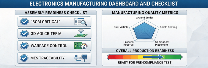
Use this list before releasing an industrial wireless design to assembly:
EMC-critical decoupling, filter and ferrite components identified and flagged in the BOM
3D AOI criteria defined for presence and offset of those components
Shield frames and cans specified with seating and corner-joint inspection requirements
Ground-connected through-hole features and QFN ground pads identified for hole-fill and X-ray review
Warpage-sensitive areas, particularly around shield frames, reviewed for fixture support
Antenna keep-out and RF zones marked on the assembly drawing
Rework restrictions agreed for shielded and filtered areas
First-article checklist extended with EMC-critical items
Approved substitution rules documented for filter and decoupling parts
Traceability level agreed, so build records can be compared if pre-compliance results vary
If you are preparing an industrial wireless design for build, PCBCart can review your files against these assembly-stage factors, including EMC-critical component verification, before production starts. Submit your project for a DFM pre-review with your BOM, assembly drawings and any list of EMC-critical parts.
Helpful Resources
• Ensuring First-Time Success in PCB EMC Design
• PCB Design for Radio Frequency Circuit and Electromagnetic Compatibility
• DFM Audit Checklist for Industrial PCBA: 38 Design Rules That Cut Rework Rate by Over 40%
• Comparison of AOI, ICT and AXI and When to Use Them during PCB SMT Assembly


