



Medical device PCBA programs carry tighter consequences for process drift than most other segments — a missed solder joint or dimensional deviation isn't just a rework cost, it's a potential field failure in a diagnostic or monitoring device. During New Product Introduction (NPI), two activities get conflated but serve different purposes: the sample build and First Article Inspection (FAI). Getting the distinction right — and structuring both correctly — is what lets a program move from prototype to production without inheriting undetected process risk.
Sample Build vs. First Article Inspection: Different Jobs

Sample build is a manufacturing readiness exercise. Its purpose is to prove the process — can this design be built repeatably with the tooling, fixtures, and parameters as specified? Sample builds typically run in small quantities (often single digits to low tens of units) and are used to validate:
· Reflow profile stability across the actual BOM (paste type, component thermal mass, PCB thickness), verified through trial runs on the JTR-1200D-N reflow oven
· Fixture fit — including whether Synthetic Stone fixtures are needed to control warpage on thin or mixed-thickness boards common in monitoring device PCBAs
· Placement accuracy on fine-pitch or mixed-technology (SMT + selective wave) assemblies
· Whether the assembly sequence itself is even viable at volume
First Article Inspection is a verification gate, not a process trial. FAI asks a narrower question: does this specific unit, built under the frozen process, conform to the released drawing and specification — dimensionally, visually, electrically, and functionally? PCBCart includes First Article Inspection as a standard value-added service on PCBA orders — one of the first completed boards is inspected and an inspection report issued before the remaining build proceeds, so errors are caught before they propagate through the batch.
The practical distinction: sample build answers "can we build this," FAI answers "did we build this correctly, and can we prove it." Treating FAI as an extension of sample build (i.e., using the same loosely-instrumented run for both) is a common failure mode — it merges process learning with conformance evidence, and when auditors or your own regulatory affairs team ask for FAI records months later, the trail is muddled.
Core Inspection Categories in FAI
For medical device PCBA, FAI should cover four categories, each with objective evidence retained. This framework goes beyond a general-purpose FAI check — it's structured specifically for the reliability demands of life sciences and diagnostic device programs:

Dimensional
· Board outline, mounting hole position/size, and connector cutout conformance against the released Gerber/drawing
· Component height clearance where enclosure fit is tight (common in handheld or wearable monitoring devices)
· Standoff and keep-out zone verification around high-voltage or isolation-critical areas
Visual (per IPC-A-610 Class 3 criteria)
· Solder joint fillet formation, wetting, and absence of voiding, bridging, or insufficient fill
· Component placement — orientation, skew, polarity marking visibility
· Conformal coating coverage and edge definition, where applicable, checked against masked/no-coat zones (connectors, test points)
Electrical
· In-circuit test (ICT) or flying probe testing against the netlist — opens, shorts, component value verification
· Functional test results where the sample build includes a test fixture
· Insulation resistance / isolation testing on boards with patient-contact or mains-adjacent circuitry, where specified by the customer's design requirements
Solderability
· Wetting angle and coverage on through-hole leads processed via selective wave (ZSWHPS-11-2 with N2 protection reduces oxidation and improves wetting consistency, particularly relevant on connectors and through-hole components common in medical monitoring PCBAs)
· Absence of solder balling, dewetting, or excess intermetallic indicators under magnified visual inspection
Using SPI/AOI/X-Ray Data During Small-Batch Trial Production
The value of small-batch NPI runs isn't just the inspection pass/fail — it's the parametric data generated along the way, which should feed back into process parameter refinement before the process is frozen for production.
3D SPI (Solder Paste Inspection) measures paste volume, height, and area at each pad post-print. During NPI trial builds, SPI data helps identify:
· Stencil aperture designs that produce marginal paste volume on specific pad geometries (common on fine-pitch or 0201/01005 components used in compact monitoring PCBAs)
· Print pressure or squeegee speed settings on the MYCRONIC jet printer/dispenser that need adjustment for a new paste type or board thickness
3D AOI, run closed-loop against SPI data, flags placement and post-reflow defects — tombstoning, insufficient fillet, component shift. In a sample build context, recurring AOI flags at the same location across multiple boards indicate a systemic issue (fixture, stencil, or placement program) rather than a random defect, and should trigger a parameter change before the next trial iteration rather than being logged and ignored.
Off-line X-ray inspection is particularly relevant for BGA and QFN packages, which appear frequently in compact medical device PCBAs where board real estate is limited. Oblique-angle X-ray capability lets engineers assess:
· Voiding percentage under BGA balls against the customer's acceptance criteria (commonly referenced against IPC-A-610 or customer-specific limits — voiding thresholds vary by application and should be confirmed with your NPI customer's engineering team rather than assumed)
· Head-in-pillow defects, which are visually undetectable but show up clearly under X-ray
The discipline here: don't treat SPI/AOI/X-ray as a pass/fail gate only. During NPI, the trend across the trial run — where defects cluster, whether they correlate with a specific panel position, feeder, or reflow zone — is the actual engineering signal. That data, tied to Smart MES traceability (UID and laser marking per unit), lets you trace a defect pattern back to a specific process input.
Sample Build Records as a Yield Baseline
One of the most commonly skipped steps: using sample build inspection results to set an expected yield baseline before production ramp — not as a contractual yield guarantee, but as an internal reference point.
A defensible baseline should document:
· Defect count and category (dimensional, visual, electrical, solderability) per unit built, tied to that unit's UID
· Which defects were process-correctable (parameter adjustment) vs. design-driven (footprint, land pattern, or component selection issue requiring an ECN)
· The process parameters in effect at time of build, so any post-launch yield shift can be compared against a known baseline rather than guessed at
This record becomes the reference an engineering team uses to ask, three months into production, "has our first-pass yield degraded, and if so, from what baseline?" Without it, that comparison isn't possible — you have current yield data and no fixed point to measure drift against.
Suggested NPI Inspection Checkpoints
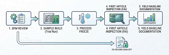
A structured checkpoint sequence for medical device NPI:
Design-for-assembly review — before any physical build, using free DFM/DFA checking to flag drill, signal/mixed-layer, power/ground, solder mask, and silkscreen issues that could affect manufacturability, alongside fixture and panelization requirements
1. Sample build (trial run) — SPI/AOI/X-ray data collected per unit, process parameters iterated
2. Process freeze — parameters locked based on sample build learnings
3. First Article Inspection — dimensional, visual, electrical, solderability checks against released drawing, on units built under the frozen process
4. FAI record sign-off — documentation package tied to UID, drawing revision, and BOM revision
5. Yield baseline documentation — defect categorization and rate logged as the pre-production reference point
If you're structuring an NPI plan for a medical device PCBA program and want to walk through how this checkpoint sequence maps to your specific design — connector-heavy monitoring device, isolation-critical sensor interface, or otherwise — request a PCB assembly quote and let us know your NPI requirements so we can scope the sample build and FAI plan against your drawing package.
Helpful Resources
· Solder Wicking on Wire Leads: The PCBA Defect That Looks Like Good Wetting
· Managing Fine-Pitch QFN/BGA Rework Risk on Medical Monitoring Device PCBA
· IPC-A-610 Class 3 Standards for High-Reliability Life Sciences Electronics Assemblies
· Traceability from Silicon to System: MES Implementation in Life Sciences Manufacturing


