



MEMS and sensor modules occupy a strange middle ground in electronics manufacturing. Unlike a digital logic board, where a passing continuity check is often enough to confirm the design intent, a MEMS or sensor module's real value lies in how accurately it measures something in the physical world — pressure, acceleration, humidity, light, or motion. A module can pass every electrical connectivity check and still fail to deliver a usable output. That gap is why device-level calibration and functional test are treated as a distinct discipline in MEMS assembly, rather than an optional add-on to standard PCBA test.
Why Device-Level Calibration and Functional Test Matter
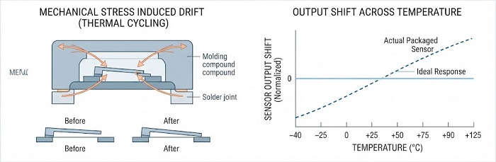
Three characteristics of MEMS and sensor devices make device-level test necessary, not just desirable.
Drift. MEMS structures are mechanical as well as electrical. Micro-scale beams, membranes, or proof masses can shift in response to thermal cycling, mechanical stress from packaging, or simple time in storage. A sensor that reads correctly at the die or wafer level may drift once it is packaged, soldered, and thermally cycled during assembly. Device-level test catches this shift before the module ships.
Unit-to-unit variation. Even sensors from the same wafer lot, assembled on the same line, can vary in offset, sensitivity, or gain due to normal process tolerances in die attach, wire bonding, or encapsulation. For many applications this variation is small enough to ignore. For applications that depend on absolute accuracy — rather than just relative or threshold-based readings — that variation needs to be measured and, in many cases, compensated for at the module level.
Environmental sensitivity. Sensor outputs are frequently a function of more than one variable. A pressure sensor's reading may shift with temperature. An accelerometer's zero-point may shift with temperature, supply voltage, or mechanical stress introduced during packaging. A humidity sensor's response curve may itself shift with temperature. If the end application operates across a range of environmental conditions, sensor behavior needs to be characterized across that same range — not just at room temperature on the bench.
General Categories of Test
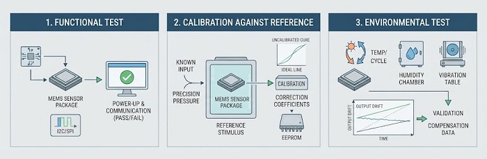
Test strategies for MEMS and sensor modules generally fall into three broad categories, often used in combination rather than as alternatives:
Functional test confirms the module powers up correctly, communicates over its interface (I2C, SPI, analog output, etc.), and produces a response to a known stimulus. This is a pass/fail gate rather than a measurement of accuracy.
Calibration against a reference compares the sensor's output to a known, traceable reference value — a reference pressure, a controlled acceleration, a certified light source — and derives correction coefficients (offset, gain, linearity) that are stored on the device or applied downstream.
Environmental test evaluates sensor performance across temperature, humidity, vibration, or voltage ranges relevant to the end application, either to validate stability or to generate compensation data for use in calibration.
Which combination of these applies depends heavily on the sensor type, the application's accuracy requirements, and whether compensation happens on-module (e.g., via onboard EEPROM) or in host-side firmware.
How This Fits Into a Broader Assembly and Test Workflow
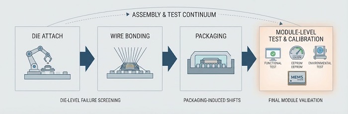
These three test categories are rarely applied in isolation — which combination runs, and at what stage, depends on where the module sits in the assembly process. Calibration and test typically sit downstream of assembly steps such as die attach, wire bonding, or flip-chip mounting, and upstream of final packaging or system integration. Because MEMS packaging can introduce its own mechanical stress, test performed only at the wafer or die level does not fully capture how the finished module will behave in the field — it screens out clear die-level failures, but packaging-induced shifts only show up once the module is assembled. That's the practical argument for treating calibration and test as part of the same continuum as assembly — planned together during NPI, not bolted on afterward.
For engineers evaluating assembly partners, the useful question isn't just "can you test this," but "how does test connect to your die-level and module-level assembly process," since the two are difficult to separate for MEMS and sensor products.
Helpful Resources
● ESD Control Protocols in PCBA Assembly for Sensitive Medical Sensor Boards
● COB on Flex and Rigid-Flex Substrates: What Changes When the Board Bends
● Fine-Pitch Wire Bonding and Multi-Chip Module Assembly: What They Enable


