



Multi-layer BGA assemblies on semiconductor Automated Test Equipment (ATE) interface boards present a specific inspection problem that standard perpendicular X-ray does not solve. When a board carries stacked or closely spaced BGA arrays across multiple layers — common in probe card interposers, DUT (device-under-test) boards, and load board assemblies — a top-down image compresses every layer into a single flattened view. The result is an inspection method that can confirm a solder ball exists but cannot reliably tell an engineer which layer it belongs to, or whether a defect sits in the layer that matters most for signal integrity and probe alignment.
This article outlines why perpendicular X-ray falls short on multi-layer ATE boards, how oblique-angle imaging addresses the gap, what Class 3 requirements add to the inspection scope, and how the resulting data should be handled downstream in a traceability system.
The Limitation of Perpendicular (0°) X-Ray on Multi-Layer BGA
A standard top-down X-ray view projects every conductive feature in the beam path onto a single 2D plane. On a single-layer BGA this is sufficient — voids, bridging, and ball shape are all visible without ambiguity. On a multi-layer board, the same projection becomes a superposition problem.
Specifically, perpendicular imaging struggles with:
Layer overlap. When BGA arrays or via structures on different layers align vertically, their images stack on top of each other, making it difficult to attribute a given void or bridge to the correct layer.
Ball-to-ball shadowing. Dense BGA pitch on ATE interface boards, where probe alignment tolerances are tight, increases the likelihood that a ball on one layer partially obscures the ball directly below it.
Ambiguous voiding attribution. IPC-A-610 voiding criteria are typically evaluated per solder joint. If perpendicular imaging cannot isolate which joint a void belongs to, the inspector is left estimating rather than measuring — undermining the acceptance/rejection decision at the joint level.
For single-layer, low-density boards, this limitation rarely matters. For multi-layer ATE interface boards — where a probe misalignment traced back to a single degraded joint can affect test yield across an entire device population — it does.
How Oblique-Angle Imaging (±15°) Separates Layer Signals
Oblique-angle X-ray inspection tilts the imaging axis relative to the board plane, typically in the range of ±15° depending on board geometry and layer spacing. This angular offset changes how features at different depths project onto the sensor.
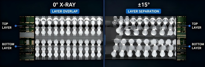
The underlying principle is straightforward: at 0°, features on different layers that share the same X-Y coordinate produce a single overlapping image. At an oblique angle, the same features are displaced laterally relative to one another in the resulting image, with the degree of displacement proportional to their depth separation (the parallax effect). This lateral separation is what allows an inspector — or an automated algorithm referencing the board's layer stack-up — to distinguish an upper-layer joint from a lower-layer joint that would otherwise be superimposed.
In practical terms, oblique-angle inspection on a multi-layer ATE board supports:
Layer-resolved void quantification. Voiding percentage can be assessed per joint per layer rather than as an ambiguous composite reading.
Isolation of bridging risk between layers. Solder bridging that would be invisible or misread under a flattened top-down view becomes distinguishable when the layers are angularly separated.
Verification of fillet and wetting geometry on the layer closest to the probe interface, which is often the layer with the tightest functional tolerance on an ATE board.
Offline oblique-angle X-ray, used as a secondary or escalation step rather than a 100% inline check, is generally the more practical deployment model — it is applied to boards flagged by 3D AOI or 3D SPI for closer joint-level review, rather than run on every unit.
Additional Requirements for Class 3 ATE Interface Boards
Semiconductor ATE interface boards — probe cards, DUT boards, load boards — are typically held to IPC-A-610 Class 3 acceptance criteria, the tier reserved for electronic products where continued performance or performance-on-demand is critical and equipment downtime cannot be tolerated. Class 3 does not change the physics of oblique-angle imaging, but it does raise the bar on what the inspection process must demonstrate:
Zero tolerance for certain defect classes. Class 3 criteria are stricter on voiding thresholds, solder ball shape uniformity, and bridging than Class 1 or Class 2. Layer-resolved imaging is what makes it possible to actually apply these stricter thresholds at the individual-joint level on a multi-layer board, rather than approximating.
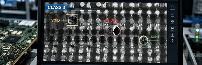
Full joint accountability. Because ATE interface boards directly affect test yield and probe alignment for downstream device testing, an inspection record that cannot account for every joint on every layer is a gap in the quality system, not just a documentation inconvenience.
Correlation with functional risk, not just cosmetic defect presence. A void that would pass under a general Class 2 read may still warrant escalation on an ATE board if its location corresponds to a probe contact point or a high-current path — this is a judgment step that requires the inspector or the review protocol to reference the board's actual layer function, not a generic checklist.
This is why oblique-angle inspection on ATE interface boards is usually paired with engineering review against the specific board's stack-up drawing, rather than treated as a pass/fail machine output alone.
Integrating Oblique-Angle Data into MES for Probe Life Tracking
Inspection data has limited long-term value if it lives only in an X-ray operator's local review station. On a Smart MES platform with UID-based traceability, oblique-angle inspection results can be tied to the individual board serial number and carried forward into the board's operational record.
This matters specifically for ATE interface boards because probe life is a degradation curve, not a fixed spec. Practical integration points include:
Per-board defect history at the joint level, referenced against the UID, so that any joint flagged during oblique-angle review is attributable to that specific board — not a lot-level average.
Baseline imaging records captured at build time, which can later be compared against field-return imaging if a board is pulled for probe degradation or contact resistance drift.
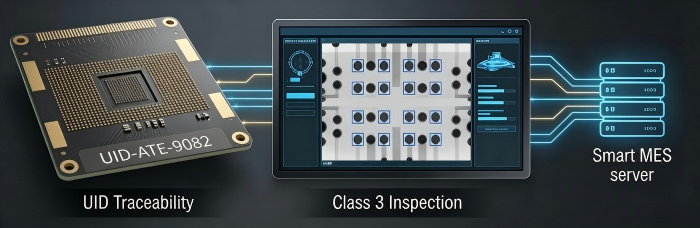
Batch-level pattern visibility, allowing a quality engineer to review whether a given defect type is isolated to one board or recurring across a build lot — a distinction that changes whether the response is a single-unit rework or a process adjustment upstream (paste printing, reflow profile, or fixture-related warpage control).
None of this requires inventing throughput or DPPM figures to be useful — the value is in the traceability linkage itself: a specific inspection image, tied to a specific UID, retrievable if that board's probe performance is later questioned.
When Oblique-Angle Inspection Is Warranted — Decision Criteria
Oblique-angle X-ray is not a default step for every board. It is justified when a board meets one or more of the following conditions:
Multiple BGA or fine-pitch layers with vertical or near-vertical alignment, where perpendicular imaging cannot separate the layers of interest.
Class 3 or functionally critical acceptance requirements, where joint-level accountability is a stated quality objective rather than a nice-to-have.
A history of ambiguous or borderline readings under standard AOI/SPI or 0° X-ray, where escalation is needed to resolve a pass/fail call with confidence rather than judgment.
Field failure attribution needs — for example, an ATE board pulled from service where engineering must determine whether a probe contact issue originated at assembly or from in-service wear.
Boards that are single-layer, lower classification, or without stacked BGA geometry generally do not need oblique-angle escalation — 3D AOI and 3D SPI closed-loop inspection, backed by standard perpendicular X-ray where voiding checks are required, remain the appropriate baseline.
Is Oblique-Angle X-Ray the Right Fit for Your Board?
If your interface board carries multiple BGA layers, requires Class 3 acceptance, or has produced ambiguous readings under standard AOI/SPI or perpendicular X-ray, oblique-angle inspection is likely warranted. PCBCart applies oblique-angle X-ray as part of its assembly-stage quality process for HMLV PCBA builds, including semiconductor ATE interface boards. Submit your board's layer stack-up and inspection requirements for a quote — our engineering team will confirm whether oblique-angle inspection fits your board before assembly begins.
Helpful Resources
● Printed Circuit Board Assembly Inspection Methods
● IPC-A-610 Class 3 Standards for High-Reliability Life Sciences Electronics Assemblies


