



Test point design is decided at the layout stage, but its consequences surface at final test — a poorly placed pad becomes a false reject, an unreachable probe becomes a coverage gap, and a coverage gap becomes a field-failure risk on a device that has no room for one. For life sciences PCBA — patient-facing monitors, diagnostic instruments, infusion and imaging electronics — test point decisions carry more weight than on general industrial boards, because an undetected defect is measured in patient risk, not just warranty cost.
Note on scope: PCBCart is IATF 16949 certified, but we do not hold ISO 13485 certification. We support life sciences PCBA assembly under our customers' own quality systems and design controls.
Why Test Point Design Deserves Its Own Review Pass

ICT (In-Circuit Test) and flying probe testing both depend on physical, repeatable electrical contact with the board. Test coverage — the share of nets and nodes actually verifiable — is a direct function of how many nodes have an accessible, correctly sized, correctly plated test point. A schematic can be functionally complete and still be untestable if the layout didn't reserve access for the test strategy.
This matters more on life sciences boards for three reasons:
Higher net density, driven by multi-channel sensing, isolation barriers, and mixed-signal (analog front-end + digital) architectures.
Higher consequence of an escaped defect — a missed solder bridge on a patient-connected circuit is a different risk category than the same defect on an industrial controller.
Longer product lifecycles, meaning the test point map often has to remain valid across multiple engineering change orders (ECOs) over years, not months.
Test Point Size, Spacing, and Plating Requirements
Pad Size and Probe Compatibility
A 1.0 mm (0.040") pad diameter is preferred for reliable contact; 0.9 mm (0.035") is acceptable; 0.8 mm (0.031") should only be used where tooling holes aid probe alignment. Smaller diameters reduce contact repeatability.
An undersized pad increases contact resistance variability — showing up as intermittent opens during test, not a hardware defect but a false reject — and accelerates probe tip wear, raising fixture maintenance frequency over time.
Avoid using vias as primary probe targets — an exposed via pad is often too small and inconsistent in shape for reliable repeated contact. Where a via must serve as a test point, keep the drilled hole to standard practice (commonly 0.36 mm / 0.014" or less) and make sure the surrounding pad still meets the same minimum diameter used for dedicated test pads.

Spacing (Pitch)
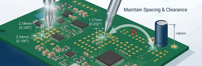
Test point center-to-center spacing must clear the mechanical envelope of adjacent probe barrels and spring housings, not just pad-to-pad electrical clearance.
2.54 mm (0.100") spacing is the commonly cited baseline, allowing standard, lower-cost probes. Tighter pitches (down toward 1.27 mm / 0.050") are achievable on dense boards but require thinner, pricier, less durable probes — often the real constraint that forces a test point redesign, more than pad size itself.
Keep pitch consistent across the full test point set rather than optimizing net-by-net; mixed pitches complicate fixture design.
If two candidate nodes are too close to both be probed, keep the one with lower observability elsewhere (e.g., a buried net) and drop the redundant one.
On the component side, keep test points clear of parts taller than roughly 5 mm (0.200") to avoid probe-to-component collision.
Plating and Surface Finish
Bare copper test pads oxidize and should be avoided on any board with meaningful time between assembly and test.
Use a controlled, solderable surface finish consistent with the incoming bare board's finish (ENIG, HASL, or equivalent) for repeatable low-resistance contact.
Test pads should not be covered by solder mask, conformal coating, or potting dam material — common on life sciences boards — unless the test point is sequenced before the coating step.
Resolving Test Point Accessibility on High-Density Boards
The nodes most useful to test (power rails, sensor front-end outputs, isolation boundary crossings) are often surrounded by the densest component clusters. Resolution approaches, in order of preference:
Reserve test access during placement, not after — keep-out zones for critical nets before component placement is locked, rather than retrofitting into a finished layout.
Use test vias on inner or bottom layers where top-side space is exhausted, provided the fixture can reach that side.
Consolidate test points logically — test a net at its most electrically meaningful, physically accessible point rather than at every trace segment.
Use boundary scan (JTAG) for genuinely unreachable nodes, such as under large BGAs<> or shielding cans, rather than accepting a coverage gap.
A defensible test strategy for life sciences PCBA is rarely 100% ICT coverage on every net — it's a documented combination of ICT/flying probe, boundary scan where applicable, and FCT for behavior structural test can't verify.
Flying Probe vs. Traditional ICT: Choosing the Right Method
Flying probe fits when:
Volume is low-to-medium, HMLV-typical — no fixture amortization to justify.
The design is still in active revision; life sciences products go through multiple ECOs during verification and validation, and flying probe needs no fixture rebuild between revisions.
Board density is too extreme for a bed-of-nails fixture to physically accommodate.
Per-unit test time isn't the bottleneck — flying probe tests sequentially, so it's inherently slower per board than ICT's simultaneous contact.
Traditional ICT fits when:
Volume is stable and the design is mature, justifying fixture cost.
Cycle time matters — ICT's parallel bed-of-nails contact tests all nodes at once.
The test point map is finalized and unlikely to change across the run.
Many HMLV life sciences programs use flying probe through NPI (New Product Introduction) and early production, then transition to ICT once volume justifies the fixture — provided the test point map was designed for both methods' access requirements from the start. Pad size and spacing should generally satisfy the more restrictive method (ICT's mechanical clearance) even if flying probe is the near-term plan.
Common Consequences of Insufficient Test Point Design
Reduced test coverage — inaccessible nodes aren't tested structurally, shifting risk onto downstream functional test or the field.
False rejects — undersized pads, tight pitch, or oxidized surfaces generate false failures, eroding yield data credibility and driving rework.
Masked real defects — inconsistent probe contact can intermittently "pass" a board with an actual solder defect, because the measurement is unstable, not the joint.
Fixture redesign cost and schedule risk — conflicts found after layout freeze force an ECO or a compromised, lower-coverage test program.
Widened variance in yield reporting, making it harder to separate real process drift from test-induced noise.
Test Point Design Checklist
Before layout freeze, verify:
Every critical net (power rails, sensor front-end I/O, isolation-boundary crossings, safety-relevant signals) has an accessible test point
Pad diameter is at least 0.9–1.0 mm (0.035"–0.040"), with smaller diameters reserved for tooling-hole-supported locations
Center-to-center spacing meets or exceeds 2.54 mm (0.100") where possible; tighter spacing is a deliberate, documented tradeoff
Test pads use a controlled, solderable finish and are clear of solder mask, coating, or potting material
Component-side test points are clear of parts taller than roughly 5 mm (0.200")
High-density clusters were reviewed for access conflicts before placement lock
Any intentionally untested node is documented with a compensating method (boundary scan or FCT)
The test point map was evaluated against both flying probe and ICT requirements, even if only one is planned near-term
Get a DFT Pre-Review Before You Freeze the Layout
Test point conflicts are far cheaper to resolve on a layout file than on a finished board. If you're finalizing a life sciences PCBA design, submit your Gerber files for a DFT (Design for Testability) pre-review — our engineering team will flag accessibility conflicts, pad/pitch issues, and coverage gaps before you commit to fixture design or production tooling.
Help Ressources
• Comparison of AOI, ICT and AXI and When to Use Them during PCB SMT Assembly
• DFM Audit Checklist for Industrial PCBA: 38 Design Rules That Cut Rework Rate
• Free PCB DFM Check and Checklist for PCB Assembly


