



Chip on board (COB) assembly is a packaging method where a bare semiconductor die is mounted directly onto a substrate — typically a PCB — instead of being housed in an individual plastic or ceramic package first. The die is electrically connected to the board and then protected with a layer of encapsulant, most often a black epoxy "blob," which is why COB modules are sometimes recognized by that characteristic dome or dot.
Because the packaging step is skipped, COB is often described as a die-level or chip-level assembly technique, distinct from surface mount technology (SMT), which places pre-packaged components (like QFNs or BGAs) onto a board.
Note: "COB" is sometimes used loosely to refer to COB LED modules — a specific lighting product built with this technique. This article covers COB as a general assembly method; LED modules are one of several applications discussed below.
What COB Means: Bare Die vs. Packaged Components
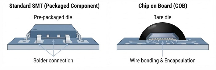
In conventional SMT, a chip manufacturer packages the die inside a protective housing with its own leads or solder balls, and that finished component is later soldered onto a PCB. The package adds a layer of protection, standardizes the footprint, and makes handling straightforward.
COB packaging removes that intermediate step. The unpackaged die — the raw piece of silicon — is attached straight to the board, wired to the circuit, and then encapsulated in place. This changes a few practical things:
Footprint: COB modules are typically smaller and thinner, since there's no separate package body.
Thermal path: With no package material between the die and substrate, heat can dissipate more directly in many designs.
Handling: Bare die are more fragile and sensitive to contamination than packaged parts, so they require controlled handling conditions.
Design flexibility: Multiple die can sometimes be placed close together on one substrate, which is useful for compact, multi-chip modules.
Because COB merges the component-packaging step and the board-assembly step into one process, it's sometimes referred to in the industry as "level 1.5 packaging" — a step between chip-level packaging and standard board-level assembly.
How COB Assembly Works (Conceptual Overview)
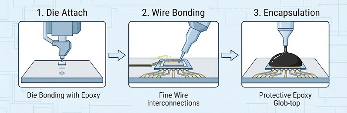
At a high level, COB assembly follows three main stages. This section describes the concept only — the finer process parameters are a separate topic.
Die attach: The bare die is bonded to the substrate, usually with an adhesive (such as conductive or non-conductive epoxy). This step secures the die mechanically and, depending on the adhesive used, may also establish an electrical or thermal connection to the board.
Wire bonding: Fine wires — typically gold or aluminum — are used to connect the bond pads on the die to the corresponding pads or traces on the substrate. This replaces the internal wiring that would normally exist inside a packaged component.
Encapsulation: Once the die and wires are connected, the assembly is covered with a protective encapsulant, commonly a glob-top epoxy. This shields the die and wire bonds from moisture, dust, physical contact, and other environmental factors, since there is no longer a plastic package doing that job.
The result is a functioning circuit where the die, its connections, and its protection are all built up directly on the board rather than assembled beforehand inside a separate package.
Where COB Is Commonly Used

COB assembly shows up most often in applications where size, thickness, or thermal performance matter more than using standardized, pre-packaged parts. Common examples include:
LED modules: COB LEDs place multiple LED chips on a single substrate under one encapsulant, producing a more uniform light source than individually packaged LEDs.
Sensors: Many sensor modules use COB to keep the sensing die as close as possible to the board, reducing size and signal path length.
Wearables: Space-constrained devices benefit from the reduced footprint and thickness that COB allows compared to packaged components.
Compact consumer modules: Products such as smart cards, small camera modules, and other space-limited electronics use COB to fit more function into less board area.
These are general, widely recognized applications of the technique rather than an exhaustive list — the right approach for any given product depends on its specific electrical, thermal, and mechanical requirements.
COB at a Glance
| Aspect | Chip on Board (COB) | Standard SMT (Packaged Components) |
|---|---|---|
| Die state | Bare die | Pre-packaged die |
| Connection method | Wire bonding | Solder (leads/balls) |
| Protection | Applied after assembly (encapsulant) | Built into the package beforehand |
| Typical footprint | Smaller, thinner | Larger, standardized |
| Handling sensitivity | Higher (bare die is fragile) | Lower (package protects die) |
In short, COB assembly is a die-level packaging approach built around three steps — die attach, wire bonding, and encapsulation — that trades some of the convenience of pre-packaged components for a smaller footprint and a more direct thermal path.
If you're evaluating whether COB fits your product and want to discuss the specifics of your design, visit PCBCart's advanced PCB assembly capabilities page to learn more about our COB and die-level assembly capabilities.
Helpful Resources
• History of High-Density Packaging Technology
• Methods Contributing to Optimization of LED PCB Design and Quality Control
• Application of Surface Mount Technology (SMT) on Ball Grid Array (BGA) Packages
• Package on Package (PoP) Assembly


