



IPC-7095D Process Guidance & IPC-A-610 Class 2/3 Workmanship Criteria | PCBCart (General Circuits) — IATF 16949 Certified PCBA Assembly
Quick-Reference Table
BGA solder joints are hidden beneath the package, so X-ray inspection — checked against a consistent void-rate reference — is the only practical way to judge them at incoming or in-process inspection. Use the table below for exactly that: pull up your X-ray report, find the row that matches your build, and compare. It's meant for manual bench comparison, not as a lookup form — cross-reference your measured void percentage against the class and application row that fits.
Formula:
Void Area % = (Total Void Area within the Solder Ball / Solder Ball Area, 2D X-Ray Projection) × 100
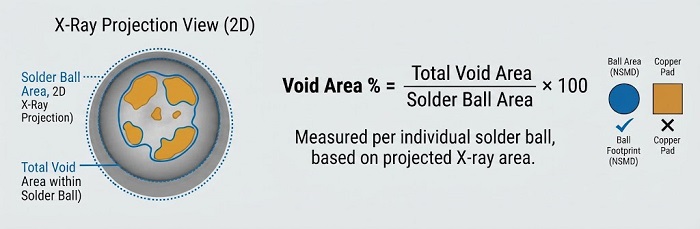
Measured per individual solder ball, referenced to the ball's own projected area in the X-ray image — not the copper pad area, which can differ from the ball footprint depending on land pattern (NSMD vs. SMD). A single ball exceeding the threshold can fail the joint even if the rest of the BGA looks clean.
| Reference Point | Numeric Basis | Governing Document | Typical Inspection Trigger |
|---|---|---|---|
| General acceptance limit (most widely cited) | ~25% void area per solder ball is the figure most commonly cited today; some references to older revisions (e.g., Rev G) cite ~30% | IPC-A-610, as commonly referenced across the industry — confirm against your current revision | Sampling AOI + X-ray on hidden-joint packages |
| Class 3 / high-reliability builds | Same general guideline applies as Class 2 — IPC-A-610 does not publish a separate, stricter void percentage by class; tighter numeric limits typically imposed by customer drawing note | IPC-A-610 Class 3 workmanship criteria (fillet, overhang, cleanliness) + IPC-7095D process guidance | 100% X-ray, oblique-angle inspection where package geometry allows |
| Semiconductor ATE interface/interposer boards | Customer-specified, commonly tightened well below the general baseline where contact repeatability under socket cycling matters | Customer drawing note referencing IPC-7095D void control guidance | 100% X-ray with per-lot correlation in MES |
| Industrial power modules | Customer-specified, focused on void location under high-current balls rather than a single blanket number | Customer drawing note + IPC-7095D thermal/void guidance | Sampling or 100% X-ray depending on criticality of the power path |
| Medical imaging boards (life sciences) | Customer-specified; we do not hold ISO 13485 and do not represent this table as a substitute for a customer's own medical-device quality requirements | Customer drawing note + IPC-A-610 Class 2/3 workmanship baseline | Typically 100% X-ray given long service life and no field-repair path |
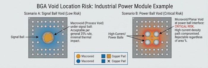
Read this table correctly: IPC-A-610 does not publish a separate void percentage for Class 2 versus Class 3 — the same numeric guideline applies across classes. The specific number also varies by revision: guidance commonly cited today lands at 25% void area per solder ball, while references to older revisions (e.g., Revision G) cite 30%. Confirm the number against your own governing revision rather than treating either figure as fixed. What genuinely changes between classes is the surrounding workmanship criteria (fillet coverage, overhang tolerance, cleanliness) and inspection coverage — Class 3 typically moves from sampling to 100% inspection. Anything tighter than the general guideline is a customer or program-specific requirement layered on the base standard, not a different IPC number.
Why the Same Void Number Passes in One Class and Fails in Another
This is the point most engineers get wrong when reading an X-ray report cold. IPC-A-610 treats voiding as one criterion among several, and it applies the same way across classes — a 22% void can pass the void metric on its own, but if the same joint shows marginal wetting or an irregular fillet, it still fails on workmanship grounds independent of the void number. IPC-7095D, for its part, is a process and inspection guide rather than a pass/fail standard: it describes how voids form, how to measure them consistently with X-ray equipment, and how to set up a sampling or control plan, then defers the formal accept/reject call back to J-STD-001 and IPC-A-610. What class assignment really changes is what gets inspected, not just the threshold — a Class 2 board may be sampled at a lot level, while a Class 3 board, or a Class 2 board carrying a Class 3 note on specific components, typically requires 100% X-ray on every BGA, surfacing marginal joints that a sampling plan would have missed entirely.
Two boards can show identical 24% readings and still get different dispositions, because one program sampled 10% of the lot and the other verified every ball. The number alone doesn't tell you the confidence behind it.
Void Morphology: Why "Percent Area" Isn’t the Whole Story
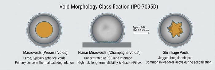
IPC-7095 defines a formal void classification (Section 7.5.3 in the current revision structure), and the practical risk differs by which category applies — not just how big the void is.
Macrovoids (process voids)
Macrovoids are the most common and most-studied void type in BGA joints — bulk voids that form in the ball, typically from flux outgassing during reflow. They're what the general ~25% (or ~30%, depending on the cited revision) acceptance guideline is written around. In power-dense designs the main concern is thermal path degradation rather than fatigue, since the joint's load-bearing cross-section usually stays largely intact.
Planar microvoids ("champagne voids")
Planar microvoids sit substantially in a common plane at the interface between the PCB land and the solder, rather than scattered through the bulk of the ball. They're often linked to surface finish issues — ENIG black pad, for instance, or entrapped cavities in certain immersion-metal finishes — rather than to the reflow profile alone. They're frequently invisible at time-zero functional test, but can seriously degrade long-term joint reliability, and they're a known contributor to head-in-pillow failure risk.
Shrinkage voids
Shrinkage voids look different from the other two — jagged and irregular rather than smooth and round. They form during the liquid-to-solid phase change, as the ball's exterior solidifies before the interior does, leaving a shrinkage cavity behind. They're more commonly reported with lead-free SAC alloys than with tin-lead.
Other categories
IPC-7095 also identifies microvia voids, caused by an unfilled via inside the land trapping gas, and pinhole voids, from entrapped fabrication chemistry reacting during reflow. Both point back to board design or bare-board fabrication rather than to the assembly process itself.
Takeaway: an "18% average" void reading without a category and location breakdown is incomplete for a reliability-driven disposition. Area percentage goes on the traveler; which category the void falls into is what an engineer actually needs to decide whether a marginal joint ships.
Industry-Specific Considerations
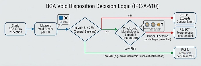
The same void percentage carries different weight depending on what the board is actually for. A few segments worth calling out specifically:
Industrial power modules
Void location under high-current balls matters more than the panel-wide average. A macrovoid under a signal ball and a planar microvoid at the interface of a power/ground ball are not equivalent risks at the same area percentage. Programs here typically write drawing notes calling out specific ball positions for tighter scrutiny rather than one blanket threshold for the package.
Semiconductor ATE interface and interposer boards
These boards see repeated socket insertion cycles in addition to thermal cycling, so contact repeatability at specific balls is often weighted as heavily as the void percentage. Void control plans here tend to reference IPC-7095D's process-characterization guidance directly, since intermittent contact resistance isn't a failure mode IPC-A-610's general void criterion was written to address.
Medical imaging boards
To be direct: PCBCart / General Circuits holds IATF 16949 certification, not ISO 13485. We do not represent our processes as meeting medical-device-specific quality system requirements, and any life-sciences customer building to that expectation should confirm their own quality system obligations independently. What we can support is IPC-A-610 Class 2/3 workmanship criteria and IPC-7095D-referenced void control on the assembly itself. Long service life and limited field-repair access are common reasons this segment specifies 100% X-ray rather than sampling — that's a customer-driven inspection decision, not a certification claim on our part.
Common Process Root Causes by Void Range (Illustrative Troubleshooting List)
Once you know where a reading falls, the next question is what's driving it. The list below is a starting checklist to narrow down a root cause before escalating — not a substitute for reviewing your own reflow profile and stencil data.
Void range 0–10% (typical/expected)
• Normal flux outgassing during reflow — expected baseline, not usually actionable
• Minor paste chemistry variation between lots
Void range 10–15% (borderline — start checking)
• Stencil aperture design (reduced/home-plate apertures can trap volatiles differently than full apertures)
• Reflow ramp rate too fast during preheat, not allowing volatiles to escape before liquidus
• Solder paste moisture uptake from extended open time
Void range 15–25% (elevated — approaching the commonly cited limit)
• Reflow soak time too short for the paste's flux system
• PCB pad or ball surface oxidation prior to reflow
• BGA package warpage during reflow, altering standoff and void escape path (synthetic-stone-fixture-supported reflow is one control point here)
• Insufficient vacuum/degas dwell where vacuum reflow capability is part of the process
Void range >25% (outside the commonly cited baseline — confirm against your governing revision)
• Stencil print volume shortfall confirmed via 3D SPI data
• Component coplanarity failure at placement
• Reflow profile fundamentally mismatched to paste alloy/flux system
• Missing or ineffective N2 atmosphere control during reflow
Cross-reference against your own 3D SPI print-volume data and reflow profile logs before treating any single X-ray reading as conclusive — a void reading in isolation, without paste-print correlation, is a symptom, not a diagnosis.
If you have an actual X-ray image showing a void condition you're trying to disposition, our applications engineering team can review it manually against IPC-7095D and IPC-A-610 criteria for your specific class and application. This is a human engineering review, not an automated tool — send the image and a brief note on your build (Class 2/3, application, package type) and we'll get back to you with an assessment.
Helpful Resources
• Automated X-Ray Inspection (AXI) for PCB Assembly Quality
• Effective Measures for Quality Control on BGA Solder Joints
• BGA Assembly Capability
• What is Ball Grid Array (BGA)


