



A board-level EMI shield is a metal enclosure fitted over sections of a printed circuit board. Its core purpose is twofold: to block external electromagnetic interference from disrupting sensitive circuitry, or to contain noisy circuits so they do not interfere with adjacent components. Since this metal cover obscures the components underneath, it introduces unique changes to PCB assembly, optical inspection and rework workflows. The most critical engineering decisions for EMI shielding are locked in during PCB layout: the shield’s mounting scheme, component placement under the shield, and its position within the assembly sequence.
What Board-Level EMI Shields Do & Why They Add Assembly Complexity
EMI shields are widely used for wireless modules, crystal oscillators, power conversion circuits and high-impedance analog circuitry — all circuits highly susceptible to electromagnetic noise or strong noise emitters. The shield forms a Faraday cage when securely bonded to the PCB ground plane. EMI shield cover assembly for emissions mitigation is a standard service offering within our PCBA assembly portfolio.
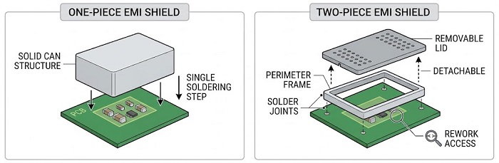
While the shielding principle is straightforward, the metal shield itself creates manufacturing overhead. Compared with standard SMT components around it, the shield has a relatively large form factor and conceals the exact circuits that require inspection and debug access. Board-level EMI shields fall into two primary designs:
One-piece shield can: Installed in a single soldering step over the target circuit area.
Two-piece shield: Consists of a perimeter frame soldered to the PCB first, paired with a removable lid that is fitted afterward.
This selection ripples through your entire manufacturing process. It defines the shield’s placement timing, whether protected circuits remain accessible post-assembly, and thermal behavior of the PCB during reflow.
Key Layout Considerations for EMI Shields
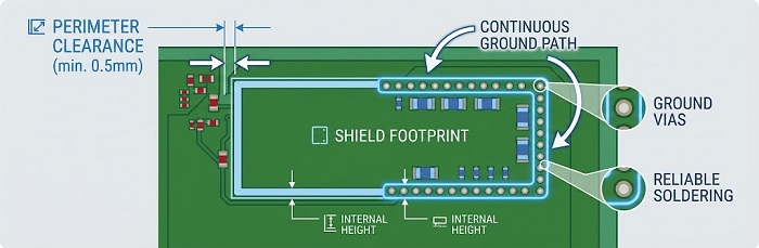
Reserve a dedicated footprint for your shield and maintain clear separation from neighboring components. Provide adequate perimeter clearance for pick-and-place placement and reliable soldering. Internal height must also be sufficient to prevent contact between the shield shell and top surfaces of enclosed parts.
If your shield grounding relies on thermal vias, place vias adjacent to mounting pads. Implement continuous grounding along the full shield perimeter — discontinuities and gaps in the ground path degrade EMI attenuation and allow noise leakage.
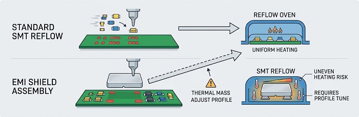
Shield height and positioning also carry practical manufacturing constraints. Tall shields placed near board edges or connectors may cause handling and mating interference. For double-sided PCBs, shields on the secondary side must account for added weight during assembly. As a substantial metal mass, shields absorb and conduct heat differently from miniature SMT components. Disclose shielding details early in your design review so we can accommodate these thermal and mechanical factors during process planning.
Consider a compact wireless PCB with a shielded radio module at one corner. If the shield footprint impinges on an adjacent connector, the connector will require relocation. If enclosed modules are not validated before lid installation, any detected fault will require shield removal for troubleshooting. Both issues are low-cost to resolve at the layout stage but lead to expensive rework on finished boards. This is why EMI shields need formal review during layout sign-off, rather than being treated as a last-minute add-on.
Preserving Inspection and Rework Access
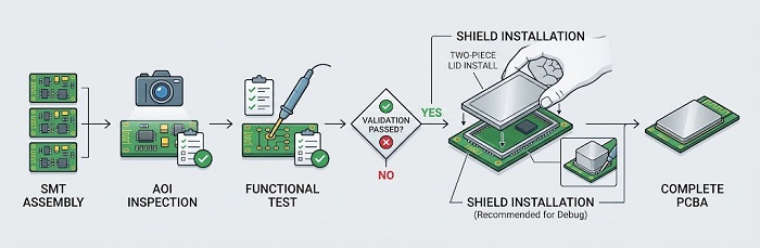
Once a shield cover is installed, automated optical inspection (AOI) cannot view covered components, and physical access for rework becomes difficult. The most practical mitigation relies on controlled assembly sequencing. Wherever your design permits, complete inspection and functional testing of circuits under the shield prior to installing the cover.
Two-piece shield designs offer a major advantage here: the lid can be detached later for debug or component replacement. One-piece cans are far less forgiving; removal requires desoldering a large metal assembly, which carries risk of pad damage or PCB delamination.
Plan your test strategy for shielded zones upfront. Locate test points, programming interfaces and functional test pads where they remain accessible with the shield assembled, or schedule full testing before shield installation. Functional testing is one of our core PCBA capabilities, and sharing your test plan lets us align the shield within your overall production flow.
Maintain simple production records for every shielded circuit block, documenting pass/fail status before the shield lid is fitted. If a unit fails in the field and the fault traces to a shielded region, this log confirms whether pre-cover testing was completed and captures original test results. Without this documentation, the only diagnostic path is shield removal — the outcome we aim to avoid. These brief notes per PCB revision add almost no overhead to your release process.
Information to Include With Your PCBA Quote Request
List the EMI shield in your BOM just like any other component, including the manufacturer part number and 2D/3D drawing. Specify whether it is a one-piece can or frame-and-lid assembly, the intended attachment method, and which PCB side the shield will be mounted on. Notify us if you will supply the shield parts consigned.
We will confirm which attachment processes our line supports for your design, as this directly sets the shield’s position in the assembly sequence. A complimentary Valor DFM/DFA check is included with our PCB assembly service. When you submit your design files, flag concerns around footprint sizing, clearance gaps and ground stitching for collaborative review.
We regularly encounter these common EMI shield design pitfalls:
Shielding untested circuits, forcing shield removal for every subsequent fault
Insufficient clearance around the shield outline, complicating placement and soldering
Omitting the shield’s thermal mass from reflow profile setup, causing uneven heating
Sparse, isolated ground connections around the shield perimeter, breaking the shielding enclosure
Frequently Asked Questions
Do you offer EMI shield cover assembly? Yes. EMI shield cover assembly for electromagnetic emission control is listed as one of our standard assembly processes.
Should I select a one-piece can or frame-and-lid shield? Frame-and-lid hardware preserves rework access to covered circuits. One-piece cans are simpler to assemble but difficult to remove. Base your selection on the expected rework or debug likelihood for your product.
Can the shield be fitted before functional testing? Technically yes, but covered circuits become difficult to inspect and troubleshoot afterward. Complete testing before shield installation whenever feasible.
Will the shield alter PCB heating during reflow? It can. Its large metal mass changes thermal distribution across the board. Identify the shield clearly in your BOM so our process team can adjust accordingly.
What documentation do I need to provide for the shield? Share the manufacturer part number, engineering drawing, attachment method and target PCB side.
EMI shields deliver the best manufacturability when footprint geometry, grounding strategy and test access are defined together, before your underlying circuit design is finalized.
Get an Instant PCB Assembly Quote
Helpful Resources
• PCB Assembly (PCBA) Workflow Overview
• Common SMT Defects & Practical Mitigation Strategies
• Complete SMT Assembly Guide to Help Cut Production Costs


