



Cellular and LoRa radio modules have become the default connectivity building block for industrial IoT sensor nodes — condition-monitoring tags, remote metering boards, asset trackers, and grid-edge telemetry devices. Most of these modules ship as pre-certified, pre-shielded system-in-package (SiP) components with fine-pitch BGA or LGA footprints, which shifts a meaningful share of the board's reliability risk onto the SMT assembly process rather than the module vendor's design. Getting the placement, reflow, and inspection strategy right on the first build is what separates a sensor board that passes field qualification from one that comes back with intermittent connectivity failures.
This article walks through the assembly-process considerations specific to cellular/LoRa module integration on industrial IoT sensor PCBAs: placement precision, coplanarity and post-reflow offset control, ground-pad void management, thermal isolation from nearby sensitive components, and firmware-batch traceability where modules are pre-programmed before mounting.
Fine-Pitch Package Characteristics and Placement Precision
Cellular modules (LTE-M/NB-IoT/Cat-1 SiPs) and LoRa transceiver modules are typically delivered in compact BGA or LGA packages, with ball/pad pitches in the 0.4–0.5 mm range and total package sizes often under 20 mm x 20 mm. A handful of characteristics drive placement risk on these parts:
Ball/pad count density — a fine-pitch BGA can carry 100+ contacts in a small footprint, so pad-to-pad clearance leaves little margin for placement offset before adjacent-pad bridging becomes possible.
Mixed contact function — RF, power, ground, and digital I/O balls are interspersed on the same grid, meaning a bridged joint is not just a cosmetic defect; it can short RF or power rails.
Component warpage tendency — small, densely populated SiPs are more prone to package warpage during reflow than larger, simpler BGAs, which compounds coplanarity concerns discussed below.
Placement accuracy for this pitch class needs to sit comfortably inside the pad's solderable window — generally interpreted as keeping X/Y offset well under 25% of pad pitch. Stencil aperture design (typically reduced aperture ratios for the fine-pitch region) and MYCRONIC jet-printed paste deposition, rather than stencil printing alone, are commonly used where paste volume needs finer control than a standard stencil can deliver across mixed-pitch boards.
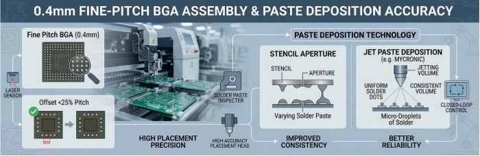
Coplanarity Requirements and Post-Reflow 3D AOI Offset Standards
Two coplanarity checks matter for module mounting, and they happen at different stages:
Before placement: PCB pad-field flatness in the module's landing area should be verified, since a locally warped board region will not let every ball make consistent contact with paste regardless of placement accuracy. Synthetic stone fixtures are used during reflow to hold panel flatness and reduce warpage-driven coplanarity drift across the thermal cycle, which is particularly relevant on boards where a fine-pitch module sits near larger, higher-mass components.
After reflow: 3D AOI is used in closed-loop with 3D SPI to check post-reflow joint geometry — not simply presence of solder, but lateral placement offset, joint height/volume consistency across the ball grid, and visible bridging risk at the array edges. For fine-pitch modules specifically, 3D AOI programming should include a tighter offset tolerance band on the module footprint than on coarser-pitch components elsewhere on the same board, since the failure mode (adjacent-ball bridging or open corner balls from warpage) is different from what shows up on a 0.65 mm+ pitch part.
Because BGA/LGA joints under a shielded module are optically obscured once the shield can is in place, 3D AOI's inspection window on these parts is effectively pre-shield: the geometry needs to be verified and signed off before the module's RF can is seated, since post-shield optical inspection is not possible.
Ground Pad Void Control and the Case for X-Ray
Most cellular/LoRa modules have a large center ground or thermal pad beneath the package — used for both RF grounding and, in some designs, as a partial heat path. This pad is the highest-risk area for solder voiding on the module footprint, for reasons consistent with any large BGA thermal pad:
Outgassing from flux volatiles has a longer escape path across a large continuous pad than across small individual ball joints.
Reflow profile ramp rate and peak temperature affect how much of that gas escapes before solidification versus getting trapped.
Paste stencil design over the ground pad (commonly broken into a grid of smaller deposits rather than one continuous print) is one of the primary levers to reduce void formation.
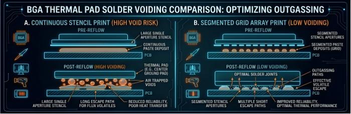
Because this pad sits directly under the package body and, once shielded, under the RF can as well, it is not visible or reachable through 3D AOI. Offline X-ray inspection with oblique-angle capability is the applicable method: oblique viewing angles let the void pattern across the ground pad be assessed rather than only a single top-down projection, which is particularly relevant when a module footprint mixes the large ground pad with smaller signal balls at different reflow depths. Void percentage thresholds for module ground pads should be defined at the DFM/process-qualification stage per module datasheet guidance, since acceptable void limits vary by thermal and RF-grounding requirements across module families.
Thermal Isolation from Antenna and Power Circuits
Cellular/LoRa sensor boards commonly place the module close to an antenna matching network, a power management section, and — critically — a crystal oscillator, either the module's own reference crystal (on modules that expose one) or a host-board crystal used for other timing functions. Reflow thermal profiling on these boards needs to account for a few interactions:
Thermal mass mismatch — the module, often the largest single component on a small sensor board, and adjacent smaller RF/passive components heat and cool at different rates, which can create localized thermal gradients across a short board span.
Crystal sensitivity — crystal oscillators are frequency-sensitive to mechanical and thermal stress; excessive or uneven thermal cycling during reflow, or thermal shock from an aggressive cooling ramp, is a recognized risk factor for frequency drift or, in more severe cases, crystal damage.
Antenna trace proximity — while antenna matching components are passive and less thermally sensitive than the crystal, keeping their reflow exposure consistent with the rest of the RF front-end reduces post-assembly RF tuning variance.
JTR-1200D-N multi-zone reflow profiling is used to manage these interactions by defining zone-specific ramp and soak parameters that limit peak temperature exposure and gradient severity across the board, rather than applying a single uniform profile across a board with mixed thermal-mass components. Where board layout allows, keeping adequate physical spacing between the module and the crystal — beyond what RF layout alone might dictate — is a DFM-stage recommendation worth flagging back to the customer's design team when reviewing Gerbers and BOM.
MES Firmware/Batch Traceability for Pre-Programmed Modules
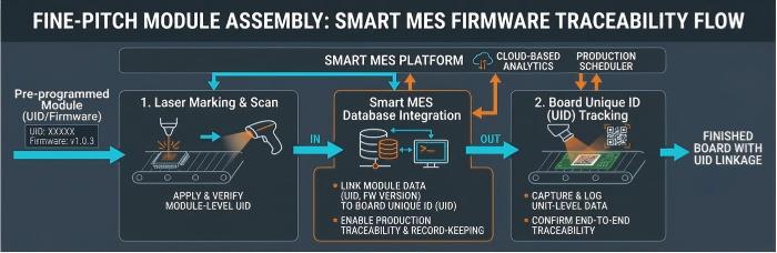
Many cellular and LoRa modules are pre-loaded with firmware or configuration profiles (APN settings, LoRaWAN keys, regional RF parameters) before mounting, either by the module vendor or via an in-line programming step prior to placement. This creates a traceability requirement distinct from standard component-lot tracking: the firmware/configuration version needs to be tied to the physical board it ends up on.
Smart MES with UID traceability and laser marking supports this by recording the module's lot and firmware/configuration version against the board's unique identifier at the point of placement, alongside the standard component-lot and process-step records already captured through the assembly line. For the OEM, this matters most after the board ships: if a subset of deployed sensors shows a connectivity or provisioning issue in the field, having firmware version and module lot linked to board serial number lets the OEM narrow the affected population to a specific batch rather than treating the entire deployed fleet as suspect.
DFM Takeaways for Module Assembly
Confirm module footprint pad pitch and ball/pad count against stencil and paste-deposition capability early in DFM review — sub-0.5 mm pitch modules may need jet-printed paste rather than stencil-only deposition.
Specify pad-field flatness/coplanarity tolerance in the module landing zone, particularly on boards where the module sits near taller or heavier components.
Break large module ground/thermal pads into segmented paste deposits rather than a single continuous print to reduce trapped-gas voiding.
Flag crystal oscillator and other thermally sensitive components in proximity to the module for reflow profile review, and consider layout spacing recommendations where feasible.
Define X-ray void acceptance criteria for the module ground pad against the module manufacturer's datasheet guidance before first-article build.
Where modules are pre-programmed, confirm the firmware/configuration version and lot are captured in MES against board UID before mounting.
Fine-pitch cellular and LoRa module integration adds process steps that a generic BGA assembly checklist doesn't fully cover — from segmented paste printing over ground pads to firmware-lot traceability. Getting these details wrong doesn't usually surface on the assembly line; it surfaces after deployment, as intermittent connectivity or provisioning failures in the field that are far more expensive to diagnose and fix than to prevent upfront.
If you're scoping a cellular or LoRa industrial IoT sensor board — whether you're still finalizing the module footprint and stackup or already have Gerbers and a BOM in hand — submitting your project details for a process capability review is the fastest way to confirm placement tolerances, void-inspection criteria, and MES traceability requirements are covered before the first build. Request a quote for your assembly project and our engineering team will follow up with DFM feedback specific to your module and board design.
Helpful Resources
• IPC-A-610 Class 3 Visual Inspection Guide for Industrial & Medical Assemblies
• Solder Paste Inspection (SPI)
• Comparison of AOI, ICT and AXI and When to Use Them during PCB SMT Assembly
• First Article Inspection Service on all PCB Assembly Orders
• Advanced PCB Assembly Services


