



Grid-tie inverter systems package power conversion and communication functions inside a shared enclosure, and increasingly on boards that sit only a few centimeters from switching devices operating at high dv/dt and di/dt. The communication board — carrying RS-485, CAN, Ethernet, or wireless telemetry interfaces back to a plant SCADA or energy management system — is the part of the system least tolerant of noise and most exposed to it. When communication drops out intermittently under load, the root cause is rarely a schematic error. It is more often a manufacturing-level detail: a shield can seated 0.2 mm off its footprint, a ground via with inconsistent fill, or a rework operation that nudged a component two millimeters from its EMI-optimized placement.
Why Communication Boards Are the Weak Link
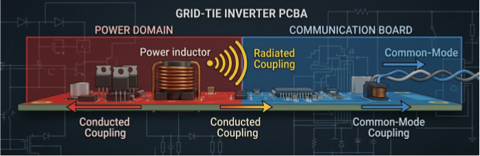
Grid-tie inverters switch at frequencies typically in the tens to low hundreds of kilohertz for the main power stage, with edge rates fast enough to generate broadband harmonic content well into the VHF range. When a communication board shares an enclosure — or worse, a PCB panel — with the power stage, three coupling paths dominate:
Conducted coupling through shared ground planes or power rails, where switching noise rides on a return path also used by low-level communication signals.
Radiated coupling from power traces and inductor near-fields into unshielded or poorly shielded communication circuitry.
Common-mode coupling through cable interfaces (RS-485 twisted pair, CAN bus, Ethernet) that act as unintentional antennas for noise present on the board's local ground reference.
Circuit designers address this at the schematic and layout level with ground plane splits, guard traces, and shielding cans over sensitive front-end circuitry (isolators, transceivers, oscillators). What determines whether that design intent survives into a shipped unit is largely an assembly-floor question.
Where Assembly Process Introduces EMI Risk
Shield can placement precision. Communication boards for inverter applications commonly specify a stamped or drawn metal shield over the isolated transceiver section and any local oscillator or crystal circuit. The shield's effectiveness depends on solder-joint continuity at all mounting tabs — a gap at even one corner reduces the shield to a partial enclosure, and near-field coupling finds the opening. Placement accuracy during reflow, not just at pick-and-place, determines outcome: a shield can that walks during reflow due to inconsistent paste volume under its tabs can land close enough to pass visual inspection while still leaving a marginal joint underneath.
Ground via process consistency. Stitching vias around a split ground plane or beneath a shield can's perimeter are frequently specified with tight pitch to maintain a low-inductance return path at the frequencies of concern. Inconsistent via fill or plating from panel to panel changes the effective ground impedance at those locations in ways that are invisible on a bare-board electrical test but relevant to high-frequency return current behavior.
Rework-induced layout disruption. This is the least discussed failure mode and often the most consequential. A communication board that requires component-level rework — a failed transceiver, a marginal solder joint on the shield itself — carries real risk of the shield can being reseated in a slightly rotated or offset position relative to its original placement, or of the rework heat profile disturbing adjacent ground-via solder. Rework procedures on EMI-sensitive assemblies need a defined shield-removal and reseating step, not an ad hoc repeat of the original placement program, because manual reseating is where positional drift enters.
3D AOI Strategy for Shield Solder Joint Integrity
Shield can solder joints are a known blind spot for standard 2D AOI, which reads primarily on solderable-area coverage and can pass a cold or partially wetted joint that presents an acceptable silhouette from directly overhead. The failure mode of concern here — a cold joint at one or more of the four shield-can corners — is fundamentally a joint-profile problem, not a coverage problem, and needs height and fillet-angle data to catch reliably.
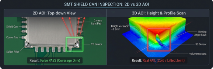
3D AOI, applied at the shield-can mounting tabs specifically, evaluates:
Fillet height and wetting angle at each corner tab, flagging joints that meet coverage but fall outside expected height/angle tolerance, consistent with a cold or disturbed joint.
Coplanarity of the shield can relative to the board surface prior to reflow completion data, useful for correlating placement drift back to paste-print or pick-and-place variance.
Post-rework re-inspection as a mandatory step, rather than an optional one, when a shield can has been removed and reseated.
This inspection strategy does not replace RF-level shielding effectiveness testing — it verifies the mechanical/solder precondition for that shielding to perform as designed. A well-formed joint at all four corners is necessary but not sufficient for shielding effectiveness; it removes assembly-introduced variance from the equation so that any residual EMI issue can be traced to layout, component selection, or enclosure design rather than a workmanship gap.
MES Traceability for EMC Pre-Compliance Support
Most grid-tie inverter programs run EMC pre-compliance testing — typically conducted by the OEM or a third-party test lab, not claimed as an in-house accreditation here — on early-build units before committing to formal certification testing. When a pre-compliance result comes back marginal on a specific emission band, the first diagnostic question is whether the tested unit is representative of the broader build, or an outlier introduced during assembly.
Smart MES with UID-level traceability is useful here specifically because it lets that question be answered with process records rather than guesswork:
Shield-can placement and reflow parameters logged per unit, so a unit sent for EMC testing can be checked against the process data for units still on the line.
3D AOI shield-joint pass/fail and measurement data tied to serial number, allowing a marginal EMC result to be cross-referenced against joint-quality data for that specific board before assuming a design-level cause.
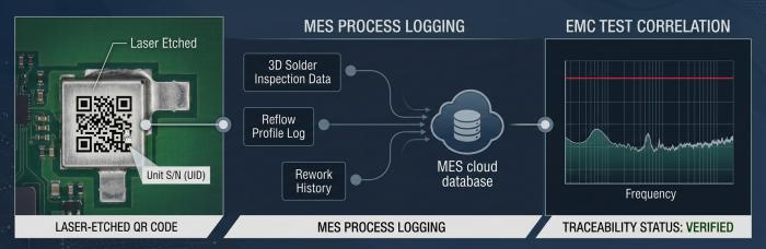
Rework history flagged per unit, so any board that underwent shield-can rework can be excluded from — or specifically included in — a pre-compliance comparison set.
This is a manufacturing-record capability, not a certification: it supports the OEM's own EMC test program by narrowing whether an anomalous result traces to a specific unit's assembly history, rather than substituting for the test itself.
EMI Risk Self-Check for Communication Board Assembly
Before releasing a grid-tie inverter communication board to production, or reviewing an existing build for intermittent field communication issues, the assembly-level checklist worth walking through includes:
Does the shield-can footprint specify solder-joint tolerance at all four corners, or only overall placement accuracy?
Is 3D AOI (not 2D) specified for shield-can joint inspection, with height/angle criteria defined rather than coverage-only?
Is there a documented rework procedure for shield-can removal and reseating, distinct from first-pass placement?
Does ground-via stitching density and plating consistency have a defined inspection or sampling plan, or is it assumed from bare-board test alone?
Is shield-joint and rework data tied to unit serial number in a way that can be pulled if an EMC pre-compliance result comes back marginal?
Most EMI issues traced to assembly rather than design come down to one of these gaps going unaddressed at the process-specification stage, not at the schematic stage.
If you're bringing a grid-tie inverter communication board into production and want these controls built into the assembly process from the start, submit your project details for a quote and our engineering team will review your shielding and grounding requirements as part of the DFM process.


