



Coplanarity Requirements for CoC Interface Boards
Chip-on-Carrier (CoC) socket boards constitute the mechanical interface between the test head and the device under test. Unlike a standard BGA assembly intended for installation within a system enclosure, the solder-side coplanarity of a CoC board directly governs contact reliability across repeated probe or pogo-pin insertion cycles.
Whereas general BGA assembly commonly tolerates coplanarity in the 100–150 μm range consistent with typical IPC-A-610 acceptance criteria, CoC interface boards intended for ATE applications typically require coplanarity below 50 μm across the full ball array — a tolerance tightened by a factor of two to three relative to conventional BGA work. This distinction is functional rather than cosmetic, for the following reasons:
Contact force distribution: Test sockets depend on uniform Z-axis compression across the entire pin field. A ball height deviation of 60–80 μm relative to the array plane is sufficient to alter local contact force enough to produce intermittent open circuits or elevated contact resistance.
Signal integrity at the socket transition: Non-uniform ball height alters effective trace length and via stub geometry at the interface, a variable of increasing consequence as ATE test frequencies rise.
Socket wear distribution: Boards with marginal coplanarity tend to accelerate socket pin wear, as contact force is not shared evenly; certain pins absorb disproportionate mechanical loading over the duty cycle of the test floor.
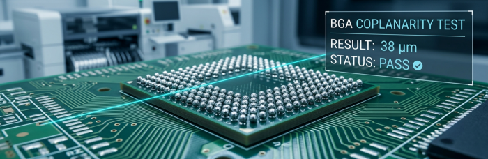
Given these functional dependencies, CoC assembly cannot be governed by standard BGA process controls alone. Process discipline must be reinforced at each stage — paste deposition, placement, reflow, and post-reflow verification — rather than concentrated solely at final inspection.
Sources of Warpage in High-Layer-Count ATE Boards
ATE interface boards are frequently constructed with high layer counts (16–24 layers or more) to accommodate dense probe fan-out routing. This construction is itself a contributing factor to warpage risk, and reflow is the process stage at which latent internal stress becomes dimensionally apparent. The principal contributing mechanisms include:
Asymmetric copper distribution: Uneven copper weight or plane density between layers produces differential coefficient-of-thermal-expansion (CTE) behavior throughout the reflow thermal ramp, resulting in board bow upon cooling.
Resin-rich versus copper-rich regions: Multilayer constructions with non-uniform resin content across the panel expand and contract at differing rates through the 235–245°C peak reflow window typical of SAC-alloy profiles.
Localized package mass effects: A high-ball-count CoC package positioned on a comparatively thin board region can induce localized "chip warpage" during the solder liquidus-to-solidus transition, superimposed on the underlying board warpage.
Inherited laminate stress: A portion of observed warpage originates not from SMT processing but from the bare laminate itself, becoming apparent only once the panel is subjected to reflow thermal cycling.
Warpage Constraint via Synthetic Stone Fixtures
To mitigate these effects, Synthetic Stone Fixtures are employed during reflow for CoC and other high-layer-count ATE assemblies. Synthetic stone — an engineered ceramic-composite tooling material — is selected specifically for its thermal mass and CTE stability relative to aluminum or standard FR4 carrier fixtures across the reflow thermal profile.
Operating parameters applied in this process include:
Full-panel support contact rather than edge-clamping alone. Fixtures are machined to match the specific board thickness and cutout geometry, constraining the panel across its full surface area rather than at the perimeter only.
Thermal ramp compatibility: Fixture mass is selected to avoid introducing thermal lag that would shift the board's local reflow profile away from the qualified curve executed on the JTR-1200D-N reflow oven.
Post-reflow dwell on fixture: Boards remain seated within the stone fixture through the initial cooling phase, as a substantial proportion of final warpage is established during solidification and the immediate post-peak cooling interval rather than the vapor phase alone.
This methodology does not eliminate warpage entirely, as the underlying CTE mismatch between materials remains a physical constraint. It does, however, constrain the panel within a repeatable dimensional envelope against which the coplanarity specification can be reliably achieved.
Two-Stage 3D AOI Inspection for Coplanarity Verification
Inspection performed only after reflow provides no opportunity for corrective action, as the assembly is already fully soldered by that point. For this reason, CoC assembly is supported by 3D AOI with laser profilometry deployed at two distinct process stages:
Post-placement, pre-reflow: 3D AOI verifies ball and paste height uniformity, along with placement accuracy, immediately following operation of the MYCRONIC jet printer/dispenser and pick-and-place equipment, prior to reflow. This stage identifies paste volume inconsistency or placement tilt while corrective rework remains straightforward.
Post-reflow: The same 3D AOI platform re-measures solder ball height and coplanarity following solidification, capturing any residual warpage introduced during the thermal process despite fixture constraint.

The principal value of maintaining both inspection checkpoints on equivalent measurement equipment lies in data correlation. Where pre-reflow paste and placement data indicate conformance but post-reflow coplanarity measurements fail specification, the defect source can be attributed with confidence to the thermal process rather than the print or placement stage. This distinction determines whether the appropriate corrective action is stencil requalification or reflow profile and fixture review — an attribution that would otherwise remain indeterminate without paired measurement data.
Oblique-Angle X-Ray Inspection for Multilayer BGA
Conventional top-down X-ray inspection is limited in its capacity to resolve stacked or closely spaced multilayer BGA packages, as solder balls belonging to different layers may overlap within the projected image, complicating attribution of voiding or bridging defects to a specific layer.
The oblique-angle capability (up to ±15°) of the off-line X-ray inspection system addresses this limitation directly:
Layer separation: Adjusting the viewing angle geometrically offsets the ball arrays of stacked packages within the resulting image, preventing upper and lower ball rows from occluding one another.
Layer-specific void quantification: Accurate measurement of BGA or QFN void percentage requires that the relevant solder ball be isolated from neighboring layers within the image; oblique-angle inspection provides this isolation for multi-die or stacked CoC-style packages.
Bridge and void disambiguation: At a straight top-down viewing angle, a bridge defect on a lower layer may visually resemble a void pattern on the layer above. The angled view resolves which layer is the actual source of the defect.
MES Traceability Linked to Probe Contact Life
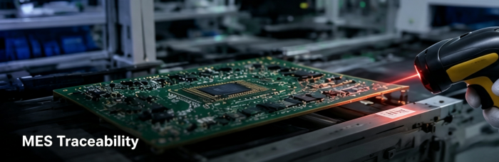
For ATE interface boards, traceability serves a function extending beyond quality documentation, informing probe and socket maintenance planning on the customer's test floor. The Smart MES platform, employing UID laser marking, associates each board serial number with the following process records:
Solder paste and ball lot data applied at the placement stage, enabling forward traceability of lot-level anomalies to specific assembled boards.
Actual reflow curve records captured per panel, as opposed to the nominal profile alone, permitting a board exhibiting premature contact degradation to be cross-referenced against its actual thermal history rather than the theoretical process specification.
This serial-number-to-process binding enables a customer's test engineering team to correlate observed probe or socket wear patterns with a specific reflow lot or solder paste batch, rather than treating each board as an undifferentiated unit within a generic production record.
DFM Recommendations for CoC and ATE Board Programs
Distribute copper symmetrically across the layer stack-up during layout design, rather than relying solely on downstream fixturing to compensate for warpage.
Specify coplanarity tolerance explicitly within the fabrication and assembly drawing, rather than referencing general IPC-A-610 criteria, to remove ambiguity regarding the tightened CoC-class requirement.
Incorporate test coupons within the panel adjacent to dense BGA regions, enabling post-reflow coplanarity sampling independent of production unit measurement.
Identify stacked or multilayer BGA locations within the fabrication drawing to enable advance programming of oblique-angle X-ray inspection paths, rather than requiring this determination during first-article review.
PCBCart supports high-mix, low-volume PCBA programs, including semiconductor test and instrumentation assemblies requiring tight coplanarity control and multilayer BGA process verification. Engineering teams developing a CoC socket board or high-layer-count ATE program are invited to submit stack-up and BGA footprint data for DFM review ahead of first build.
Ressources utiles
• Free DFM Pre-Review
• PCB Testing Methods Guide
• Elements to Consider in BGA Assembly Process Capability
• Components Sourcing & Management
• Contact PCBCart's Engineering Team


