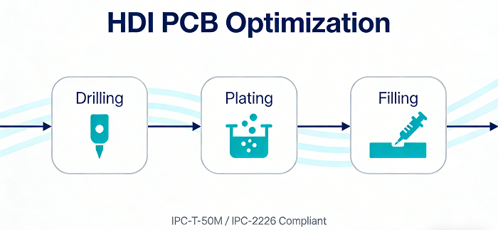
High-density interconnect (HDI) printed circuit boards are for high-performance and miniaturized electronics, and have become the workhorse in everything from smartphones to complex aerospace systems. At the heart of HDI PCB performance is the precision of microvias, those tiny laser-drilled holes that allow reliable layer-to-layer connectivity in dense designs. Moreover, to ensure superior electrical performance, structural integrity, and manufacturability, unlocking HDI PCBs' full potential requires optimization of three crucial processes: microvia drilling, copper plating, and filling. This article begins to discuss actionable strategies to refine each step by drawing on industry standards, advanced techniques, and best practices from PCB manufacturing expertise.
1. Optimizing Microvia Drilling: Precision, Material Compatibility, and Defect Prevention

Microvia drilling is basically the foundation of HDI PCB design. Minor inconsistencies in this process may compromise subsequent plating and filling processes. To get the best performance, HDI PCB manufacturing should embody precision, material selection, and strict adherence to standards.
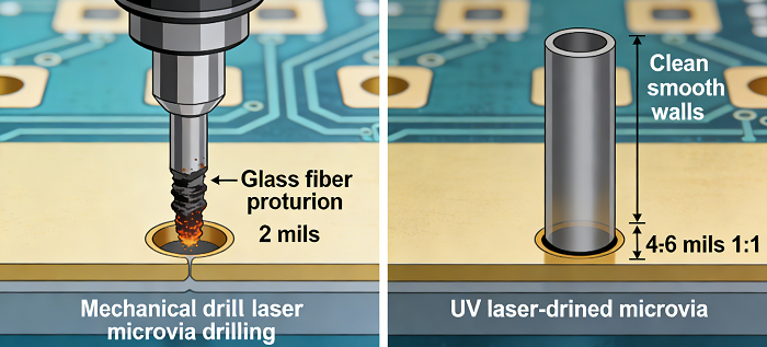
Define microvias to IPC specification. The typical microvia, as defined by the IPC, would have an aspect ratio of 1:1, maximum depth of 0.25 mm (0.010 inches), and its diameter ranges between 4 and 6 mils. Greater than a 1:1 aspect ratio increases the chance for reliability problems like non-uniform plating or barrel cracks; therefore, for high-reliability applications, a more conservative aspect ratio ≤0.8:1 is desirable. The preferred method for forming microvias involves laser drilling. It boasts up to 99.3% accuracy, unmatched by mechanical drilling. For very small diameters and thin dielectric layers, laser drilling remains unparalleled. Advanced laser systems minimize damage due to heating effects, reducing resin smear and glass fiber protrusion. This makes defects in these two common problems less likely, which can compromise plating adhesion.
The success in drillability begins with material selection: select only laser-compatible dielectric materials with flat or spread glass structures. Examples include a high-quality resin system specifically designed for use with laser drilling, or non-reinforced build-up films. These provide consistent laser ablation to prevent uneven via tapers and charring of the material. Materials containing mismatched thermal expansion rates should be avoided, for they can cause misregistration between the capture pad and the target pad during the drilling process. Additionally, ensure stack-up homogeneity-mixing materials of different laser energy absorption rates creates an inconsistent quality in drilling. High-resin or low-profile glass cloth types (1035, 1067, 1086) will allow for better ablation uniformity and minimal smear.
The pre-drilling job and post-drilling cleaning should be given equal importance. Substrate surfaces should not have contamination to allow for drill wandering. Once drilling is done, after proper plasma etching or a special cleaning procedure is applied, resin smear and debris need to be removed, especially for the 2-HDI boards and complex 6-layer designs. This process eliminates any barrier to copper adhesion and reduces risk in void formation in the plating subsequents.
2. Copper Plating Optimization: Homogeneity, Adhesion, and Rel

Copper plating is a process used in microvias interconnections. The quality of the copper plating process affects the signal integrity as well as the ruggedness of the interconnections. The copper plating process must be optimized through the proper combination of copper plating methods, parameters, as well as manufacturing.
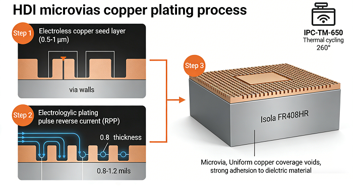
Begin with a sound pre-plate base—electroless copper plating. This technology provides a thin, uniform layer, usually 0.3 to 0.6 mils, on the walls of holes for full coverage on microvias. Effective preparation for plating is paramount to good adhesion; otherwise, plating can readily delaminate with contamination present on the walls of holes.
Select the appropriate electroplating method based on the design requirements:
· Wrap Plating: This type of plating, used optimally to provide improved interconnectivity between layers, coats copper on the sides of vias, extending copper into surface pads. It translates to high mechanical strength but demands precision to prevent excessive copper deposition, impacting the positioning of fine-pitch components.
· Button (Spot) Plating: The process favors deposition of copper in the form of via holes and pads, reducing the overall copper present on the surface of the PCB. It is very useful in PCB designs involving the need for effective control over the thickness of the barrel of the via hole.
· Pulse/Reverse Pulse Plating (RPP) vs. DC Plating: RPP plating, which offers improved copper distribution compared to DC plating, enhances copper distribution, which becomes even more important in the case of thick substrate PCBs and stacked MicroVia structures. RPP prevents clogging of pastes in the holes.
Process parameters can be optimized to minimize potential problems such as inhomogeneous deposition. Current density (reduced for smoother deposit but increased for increased production rate), stirring rate (helps in uniform distribution of the solution), and temperature can be controlled. The plating process should involve semi-automatic or automatic plating equipment offering submicron precision (±0.1 µm). The copper thickness should ideally vary from 0.8 to 1.2 mils, which is an ideal tradeoff for conductivity and manufacturability. In addition, anodes and plating agents, such as leveling agents, should be of good quality to minimize impurity and smooth the surface.
IPC specifications should be followed for plating reliability. Make sure that the target pad size is at least 80% of the via size to avoid concentration of stress and that there should be no clearance between the solder mask and microvias to avoid solder wicking during reflow. Monitor the resistance test after thermal cycle testing as per IPC-TM-650 2.6.27 specifications with no more than 5% change in maximum allowable resistance.
3. Optimizing the Filling of Microvias in Printed Boards through Flatness

Microvia filling removes voids, improves mechanical robustness, and allows planarity for components such as BGAs. Whether to fill or avoid microvias using copper or resins is based on their usage and type, but optimization is in applying techniques that aim for planarity, defect reduction, and convergence with the design requirements.
Step 1: First, determine the type of filling that
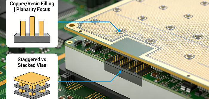
· Filled Microvias: Via-in-pad and buried microvias must be filled. Copper filling is necessary to avoid voids under the copper which cause stress concentrations during the reflow soldering cycle. However, filling with resin reduces signal delay and increases planarity. The processing includes placing a layer of conformal plating over the microvias followed by a pulsed layer of copper.
· Unfilled Microvias: usable in non-critical blind vias not utilized in component pads, but in modern high reliability designs they have been almost eliminated.
Emphasis on flatness for enhanced designs. Incomplete filling will result in dimples, which can be detrimental to the quality of the solder joint in fine pitched designs. Semi-Additive Processes, mSAP, for instance, rely on the use of copper foil to provide flatness suited for stacked via and via in pad designs. Planarization of the board after filling provides the needed flatness, which, when lacking, causes solder ball defects in BGA packages.
Overcome filling challenges by optimizing processes and leveraging technology. Employ simulation software to simulate and lessen taper issues by optimizing cathode size and varying thickness to limit taper by up to 40%. To improve filling in laser-drilled holes, overcome damages caused by heating by incorporating hole cleansing before filling, where ash inside holes prevents filling. Employ new plating solutions and equipment to optimize filling rates with less cost and effort.
Carefully balance flexibility in the design and the cost involved in implementation. Staggered microvias cost less to fill compared to stacked vias, and they also result in better robustness against thermal stress. Stack no more than two layers in microvia structure; for more than two, it is advised to use staggering. If there is enough room, skipped vias, which are mechanically drilled, become an inexpensive alternative for laser-drilled stacked vias for multi-layer connections.
Conclusion

Optimizing microvia drilling, copper plating, and filling is an integrated and careful task that involves great attention to material, process, and industry standards. Utilizing the abilities of laser drilling, pulse plating, and selective filling enables the fabrication of HDI PCBs capable of handling the miniaturization and functionality associated with next-generation electronics. Strict cooperation with standards such as IPC-T-50M and IPC-2226 ensures that all designs are not only possible to manufacture but also reliable and free from defects. Process monitoring from drilling to resistance reflow enables the correction of inherent and potentially unnoticed manufacturing defects and thus ensures optimal functionality of the resulting HDI PCBs.
Helpful Resources
• 3 Keys to Designing a Successful HDI PCB
• Factors Affecting the Quality of BGA Assembly
• Solving Signal Integrity Issues in HDI PCBs
• Acceptance Criteria of IPC-A-600 in PCB Manufacturing
• Common Defects in PCB Assembly and How to Prevent Them


