



High-Density Interconnect (HDI) printed circuit boards are an essential part of modern electronics manufacturing, as they are increasingly being used in smaller and more complex devices with higher processing speeds. The possibilities range from smartphones and wearable electronics to automotive control systems and medical electronics, to compact, high performance PCB layouts that are not possible with traditional boards.
But creating HDI PCBs includes a number of challenges for manufacture and reliability. One of the most important (but frequently overlooked) is solder mask clearance. The design of solder mask has a direct influence on the precision of the assembly, reliability of solder joints, product electrical insulation and the long-term workability of the product.
In ultra-dense PCB environments where trace widths and spacing are measured in microns, even slight solder mask misalignment or insufficient clearance can lead to significant manufacturing defects and operational failures.
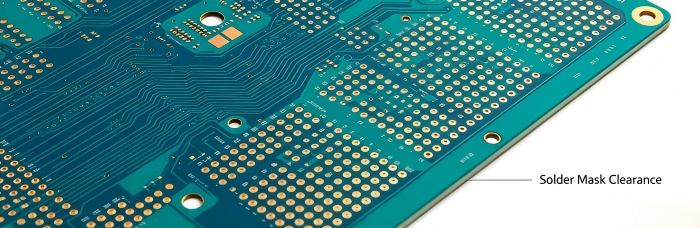
What Is Solder Mask Clearance?
Solder mask clearance is defined as the distance between the edge of a copper feature, like a pad, via or trace, and the edge of the solder mask opening around the copper feature. Actually, the solder mask is a thin layer of protective polymer that is placed on the top of the PCB to provide an electric isolation layer between the copper circuits and to avoid unwanted soldering while the boards are being assembled.
By exposing the copper area created in the solder mask opening, components can be soldered to the board, leaving the exposed conductive area protected by the surrounding mask.
In HDI PCB designs, solder mask clearance plays a particularly significant role in the fact that the distance between conductive features is very small. Proper mask registration and clearance is important for manufacturability and electrical reliability.
Why Solder Mask Clearance Matters in HDI PCB Design
Preventing Solder Bridging and Short Circuits
Fine pitch components like BGAs, CSPs and microvias are frequently used in HDI boards. Usually, these packages will also include a gap of less than 0.5 mm between the pads, which will make the assembly easier.
Where there is a large gap for solder mask, there can be excessive exposure to the copper and solder bridging between connecting pads may become possible during reflow. On the other hand, a small clearance can cause the solder mask to overlap the pads on the board because of registration tolerances, which can cause issues with solderability and component attachment.
The effective separation achieved by well-controlled solder mask openings also helps to lower the chance of short-outs and enhance assembly rates.
Improving Solder Joint Reliability
From a mechanical and electrical perspective, reliable solder joints are required for the overall stability of the HDI assemblies. The poor design of solder mask can cause solder paste not to adhere to the components or poor solder wetting.
If solder mask creeps up on to pads, the soldering joints may not be uniform, causing the mechanical bond to be uneven or electrical connection to be inconsistent. These defects over time can cause intermittent failures, or poor product life, or thermal fatigue.
The uniform solder flow and the resulting stronger and more reliable interconnections are a result of optimized solder mask clearance.
Supporting High-Precision Manufacturing
Advanced processes like laser-drilled microvias, sequential lamination, ultra-fine traces and stacked via structures are used for modern HDI fabrication. With the rise in precision and accuracy of fabrication equipment, solder mask alignment continues with the use of manufacturing tolerances.
The typical solder mask registration tolerances are ±2 mils to ±3 mils depending on the ability of the fabrication process and the complexity of the board. In ultra-HDI structures these tolerances are very important.
These variations should be taken into consideration when laying out the designs. Clearance margins less than the desired tolerances may lead to solder mask overlap on pads, or unwanted exposure to copper which can negatively impact manufacturability.
The Relationship Between Solder Mask and Fine-Pitch Components
The higher the component density, the more challenging it is to keep solder mask dams in place. The length of solder mask material between adjacent pads which prevents solder bridging is called a solder mask dam.
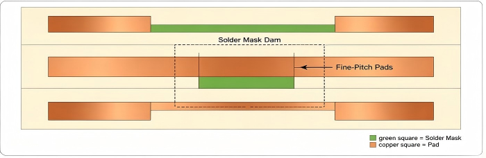
In certain very fine-pitch devices, space is limited for use of traditional solder mask dams. In these instances, manufacturers can offer variations in design as needed for fabrication and assembly.
To optimize electrical performance and ensure manufacturability, fine-pitch HDI layouts demand close collaboration among the PCB designer, fabricator and assembly engineer.
Solder Mask Defined vs. Non-Solder Mask Defined Pads
In HDI PCB manufacturing, there are two popular approaches for designing the pads:
Non-Solder Mask Defined (NSMD) Pads
NSMD designs have the opening in solder mask slightly larger than the copper pad, so that the entire copper surface and pad edges are exposed. Typically, this structure provides improved solder wetting and solder joint reliability.
Fine pitch BGA applications are usually preferred to use NSMD pads since they form more consistent solder joints.
Solder Mask Defined (SMD) Pads
If the solder mask opening in SMD design is smaller than the copper pad, the part of copper pad edge will be covered by solder mask. This can be useful, if a lot of solder space is restricted; however, it can also affect the geometry of the solder connections and their stress distribution.
NSMD or SMD structures are chosen based on the type of component, its pitch size, the density of the board and manufacturing limitations.
Common Challenges in HDI Solder Mask Design
Solder Mask Misregistration
A slight deviation from alignment may reveal copper, or partially obscure solderable areas. For HDI boards, which have a very tight spacing, registration accuracy becomes crucial.
Reduced Solder Mask Dam Width
With the reduction of trace/pad spacing, solder mask dams prove to be harder to maintain. Narrow width of the dam may lead to solder bridging during assembly.
Ultra-Thin Trace and Microvia
HDI boards can include laser drilled microvias and traces under 3 mils in thickness. The miniatures demand extremely controlled processes for solder mask application in order to ensure dimensional stability.
Thermal and Mechanical Stress
Stress can be focused around solder joints due to poor solder mask design, particularly when thermal cycling, vibration or mechanical flexing is used.
Best Practices for Optimizing Solder Mask Clearance
The following are a few tips that should be followed by PCB designers to make this an easy and reliable task with improved manufacturability and HDI:
Adhere to IPC standards/recommended design guidelines by manufacturers
Determine solder mask clearances to meet actual fabrication tolerances
Do not excessively aggressively space down in fine pitch areas
Check with the PCB manufacturer the minimum solder mask dam size
Apply Design for Manufacturability (DFM) Analysis at the beginning of the design
Test prototypes prior to mass production
In coordination, design solder mask in accordance with stencil and assembly process requirements.
For advanced high density interconnect applications use high resolution LPI (Liquid Photoimageable) solder mask materials.
Emerging Trends in Ultra-HDI Solder Mask Technology
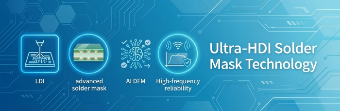
However, the classic solder mask processes are rapidly changing as PCB technology moves toward ultra-high density structures and semiconductor-like packaging densities.
Emerging developments include:
Laser direct imaging (LDI) for improved mask registration accuracy
Materials for advanced photoimageable solder mask
Solder mask is processed using a finer resolution process
AI-assisted DFM optimization
Improved reliability testing for high-frequency and high-speed applications.
These innovations enable the manufacturers to get closer to tolerances and have a reliable assembly in the present electronic products, which are becoming more and more compact.
It is a fundamental part in HDI PCB design which directly affects manufacturing precision and assembly yield, electrical performance and the long-term reliability of products. With today's high-density electronics, where spacing between components is shrinking, it has never been more important to have the correct solder mask design.
Engineers can minimize defects in PCB assembly and enhance the performance of their printed circuit boards by carefully optimizing solder mask clearances, ensuring proper solder mask dams and considering fabrication tolerances.
With the ongoing evolution of HDI technology, manufacturers and designers need to use the tools and technology necessary to support the next generation of electronic systems that are becoming ever smaller and faster.
PCBCart offers advanced and assembly PCB fabrication capabilities, strict quality control processes, and professional engineering support for demanding high-density applications. Whether you require fine-pitch PCB manufacturing, microvia technology, or customized HDI solutions, PCBCart can help streamline your production process while maintaining high reliability and cost efficiency.
Helpful Resources
• How to Optimize Microvia Drilling, Copper Plating, and Filling for HDI PCBs?
• 3 Keys to Designing a Successful HDI PCB
• PCB Fabrication Tolerances What You Need to Know
• How to Inspect and Test Solder Mask Quality on PCBs?
• PCB Design for Manufacturability Guidelines
• Free DFM Check Before Production


